| Jul 03, 2023 |
|
(Nanowerk Information) The quick switching and modulation of sunshine is on the coronary heart, amongst different issues, of contemporary knowledge switch, through which info is distributed by means of fibre optic cables within the form of modulated mild beams. It has been potential for a number of years now to miniaturise mild modulators and to combine them into chips, however the mild sources themselves – mild emitting diodes (LEDs) or lasers – nonetheless pose issues to engineers. A staff of researchers at ETH Zurich led by Prof. Lukas Novotny, along with colleagues at EMPA in Dübendorf and at ICFO in Barcelona, have now discovered a brand new mechanism by which tiny however environment friendly mild sources could possibly be produced sooner or later.
|
|
The outcomes of their analysis have lately been revealed within the scientific journal Nature Supplies (“Exciton-assisted electron tunnelling in van der Waals heterostructures”).
|
Making an attempt the surprising
|
|
“To attain this, we first needed to attempt the surprising”, says Novotny. For a number of years he and his coworkers have been engaged on miniature mild sources which are based mostly on the tunnel impact. Between two electrodes (manufactured from gold and graphene on this case) separated by an insulating materials, electrons can tunnel in line with the foundations of quantum mechanics. Beneath explicit circumstances – that’s, if the tunnel course of is inelastic, which means that the power of the electrons just isn’t conserved – mild could be created.
|
|
“Sadly, the yield of these mild sources is relatively poor as a result of the radiative emission may be very inefficient”, explains postdoc Sotirios Papadopoulos. This emission downside is well-identified in different areas of know-how. In cell phones, as an illustration, the chips that create the microwaves wanted for transmission are just a few millimetres in dimension. In contrast, the microwaves themselves have a wavelength of round 20 centimetres, which makes them 100 instances bigger than the chip. To beat this distinction in dimension an antenna is required (which, in fashionable telephones, is definitely now not seen from the surface). Likewise, within the experiments of the Zurich researchers the wavelength of the sunshine is way bigger than the sunshine supply.
|
Semiconductor outdoors the tunnel junction
|
|
“One would possibly suppose, then, that we had been consciously searching for an antenna answer – however in actuality we weren’t”, says Papadopoulos. Like different teams earlier than them, the researchers had been investigating layers of semiconductor supplies resembling tungsten disulfide with a thickness of a single atom sandwiched between the electrodes of the tunnel junction as a way to create mild on this manner. In precept one would assume that the optimum place ought to be someplace between the 2 electrodes, possibly a bit of nearer to at least one than to the opposite. As an alternative, the researchers tried one thing fully totally different by placing the semiconductor on high of the graphene electrode – fully outdoors the tunnel junction.
|
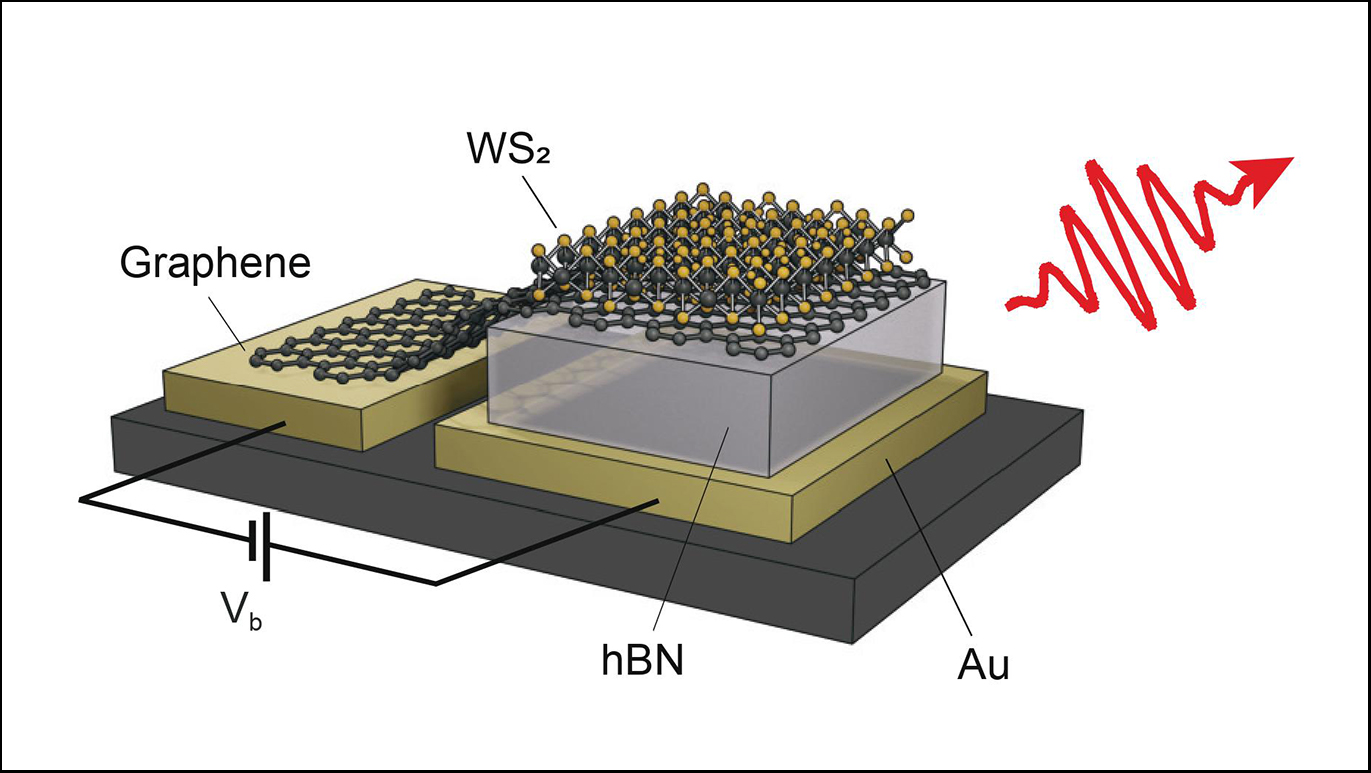 |
| The semiconductor materials (tungsten disulfide, WS2) positioned outdoors the tunnel junction (proper) acts as an antenna and makes it potential to reinforce the power created within the tunnel junction. (Illustration: Sotirios Papadopoulos / ETH Zurich)
|
Shocking antenna motion
|
|
Surprisingly, this apparently illogical place labored very effectively. The researchers came upon the explanation for this by various the voltage utilized to the tunnel junction and measuring the present flowing by means of it. This measurement confirmed a transparent resonance, which matched a so-called exciton resonance of the semiconductor materials. Excitons are manufactured from a positively charged gap, which corresponds to a lacking electron, and an electron sure by the outlet. They are often excited, as an illustration, by mild irradiation. The exciton resonance was a transparent signal that the semiconductor was not excited instantly by cost carriers – in any case, there have been no electrons flowing by means of it – however relatively that it absorbed the power created within the tunnel junction and subsequently re-emitted it. In different phrases, it acted very very like an antenna.
|
Purposes in nanoscale mild sources
|
|
“For now, this antenna just isn’t excellent as a result of contained in the semiconductor so-called darkish excitons are created, which implies that not a lot mild is emitted”, Novotny concedes: “Enhancing this can be our homework for the close to future”. If the researchers are profitable in making the sunshine emission by the semiconductor extra environment friendly, it ought to be potential to create mild sources that measure just a few nanometres and are, thus, a thousand instances smaller than the wavelength of the sunshine they produce. As there aren’t any electrons flowing by means of the semiconductor antenna, there are additionally not one of the negative effects that usually happen at boundaries and that may cut back the effectivity. “In any case, we’ve got opened a door to new functions”, says Novotny. Making an attempt the surprising has evidently paid off.
|
