| Jul 04, 2023 |
|
(Nanowerk Information) Nanometer-scale coatings with useful supplies play an necessary function in lots of sensory, digital and photonic functions. A global crew of researchers – coordinated by Leibniz IPHT in Jena, Germany – has succeeded for the primary time in observing novel progress results of tin coatings on silicon nanometer-structured surfaces. With the data gained, the chemical composition of deposited skinny movies could be exactly managed and monitored sooner or later, opening up new functions within the fields of biophotonics, vitality technology or mobility.
|
|
The outcomes have been printed within the journal Small (“Spectromicroscopy Research of Silicon Nanowires Array Coated by Tin Oxide Layers” and “Nanostructured Silicon Matrix for Supplies Engineering”).
|
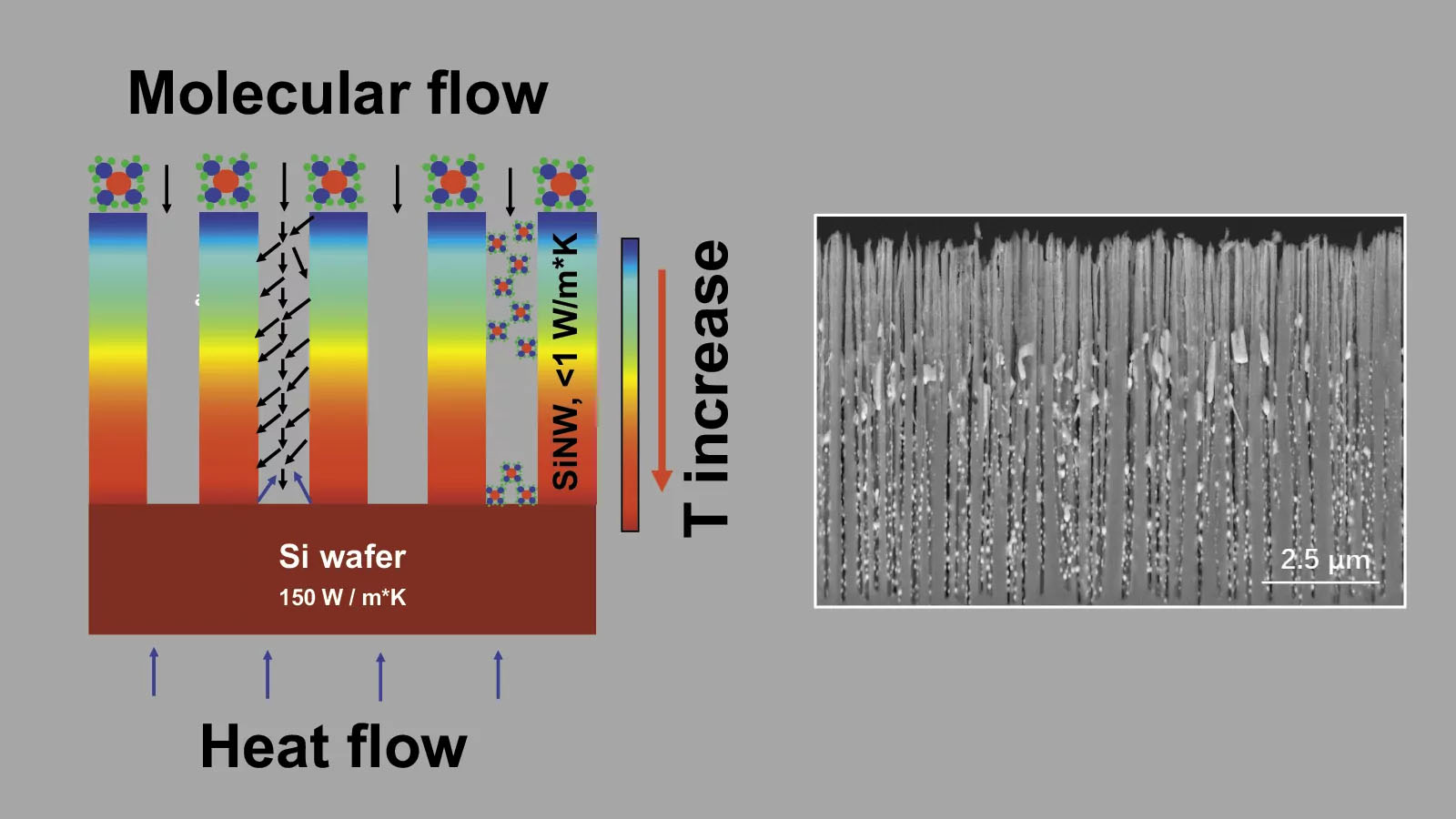 |
| Dynamics of the molecular precursor within the nanochannel throughout the MOCVD course of (left within the image) and typical SEM cross-sectional view of the nanostructured silicon matrix after coating (proper within the image). (Picture: Leibniz IPHT)
|
|
Tin-containing layers are in demand for all kinds of digital elements and elements within the electrical trade in addition to in sensor know-how or photovoltaics. Researchers from the Leibniz Institute of Photonic Know-how (Leibniz IPHT) investigated the event technique of nanoscale tin layers along with scientists from Germany, Russia and Nice Britain and summarized their ends in the famend journal Small.
|
|
The beginning materials for the noticed progress processes of tin-containing skinny movies are ultra-thin silicon-based buildings within the type of nanowires with a diameter of lower than 100 nanometers. In experimental research, the researchers have been capable of exhibit for the primary time a selected distribution impact of tin alongside these silicon nanostructures: Tin-containing layers with totally different levels of oxidation have been shaped alongside all the size of the semiconductor nanowires by way of metal-organic chemical vapour deposition at a deposition temperature of 600 levels Celsius.
|
|
„By understanding how tin coatings develop and which components affect this progress course of, we create the situations for particularly controlling coating processes. This permits surfaces to be refined very exactly and to be outfitted with desired useful properties at beforehand outlined positions,“ explains Dr. Vladimir Sivakov, head of the Silicon Nanostructures Group at Leibniz IPHT, who investigated and found the expansion mechanisms collectively together with his crew.
|
Functions of ultra-thin tin layers
|
|
Nanometer-thin coatings with tin allow particular optical and electrical properties and permit, amongst different issues, to additional enhance the analysis and growth of optical and biophotonic strategies. Tin layers can be utilized as UV-SERS-active surfaces in surface-enhanced Raman scattering (SERS) spectroscopy, which could be utilized to find out the molecular fingerprint of organic samples utilizing SERS-active steel nanostructures. As well as, there are areas of utility in fuel sensors through which tin reacts to gases as a extremely delicate layer. Software eventualities in high-performance lithium-ion batteries for electromobility and thermal vitality storage are additionally conceivable, through which tin-coated anodes guarantee excessive digital conductivity.
|
Mechanisms and progress dynamics of tin-containing layers
|
|
The researchers investigated the expansion dynamics of the noticed tin-based layers on nanostructured surfaces utilizing microscopic and spectroscopic strategies. In distinction to planar and unstructured silicon surfaces, on which the deposition happened homogeneously, the surfaces of the semiconductor nanowires have been lined with tin-containing crystals of various styles and sizes over all the size.
|
|
The outcomes offered within the journal Small present the formation of various tin oxide phases alongside the nanostructured silicon surfaces, which might be recognized with tin dioxide (SnO2) within the higher half, tin monoxide (SnO) within the center half and with metallic tin (Sn) within the decrease half.
|
|
The quantity and distribution of the shaped metallic Sn and its SnO and SnO2 oxides could be defined and successfully managed by the size, diameter, porosity, and spacing of the silicon-based semiconductor nanostructures. Along with these geometrical parameters, the researchers have been capable of reveal the formation of hydrocarbon-containing by-products as decreasing brokers for tin oxide discount as one other issue influencing the distribution of the shaped tin layers alongside the semiconductor nanostructures. The thermal conductivity of the silicon buildings and thus the temperature distribution alongside the nanowires throughout the high-temperature vapour deposition also can have an affect on the formation of various tin oxide phases.
|
