| Jul 13, 2023 |
|
(Nanowerk Information) Researchers have demonstrated a steady curler printing course of that may decide up and switch over 75,000 micrometer-scale semiconductor units in a single roll with very excessive accuracy. The brand new technique paves the best way to creating large-scale arrays of optical parts and might be used to quickly manufacture micro-LED shows.
|
|
Micro-LED show know-how is of nice curiosity as a result of it may possibly accomplish extremely correct colour rendering with excessive pace and backbone whereas utilizing little energy. These shows may be utilized in a variety of codecs together with smartphone screens, digital and augmented actuality units and enormous shows a number of meters throughout. For bigger micro-LED shows, specifically, the challenges of integrating hundreds of thousands of tiny LEDs — that are typically smaller than a grain of nice sand — onto an digital management backplane are monumental.
|
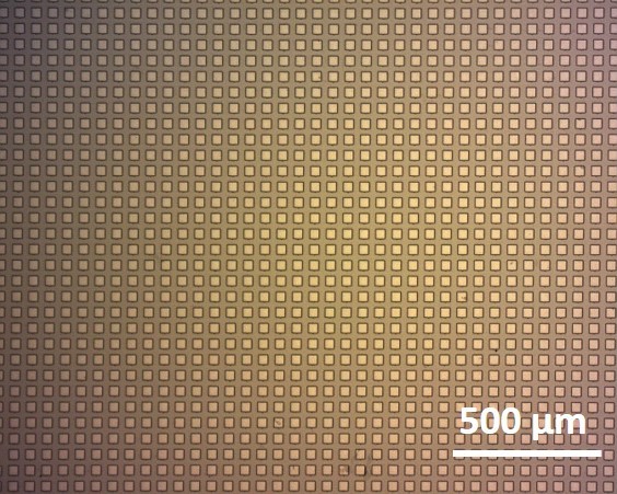 |
| Researchers developed a steady curler printing course of that may decide up and switch over 75,000 micrometer-scale semiconductor units in a single roll with very excessive accuracy. An optical microscopy picture of the curler switch printing outcomes is proven. (Picture: Eleni Margariti, College of Strathclyde)
|
|
“Transferring micrometer-scale semiconductor units from their native substrate to quite a lot of receiving platforms is a problem being tackled internationally by each educational analysis teams and industries,” mentioned analysis crew chief Eleni Margariti from the College of Strathclyde within the UK. “Our roller-based printing course of presents a strategy to obtain this in a scalable method whereas assembly the demanding accuracy essential for this software.”
|
|
Within the journal Optical Supplies Specific (“Steady curler transfer-printing and automatic metrology of >75,000 micro-LED pixels in a single shot”), the researchers report that their new curler know-how can match the designed system structure with an accuracy of lower than 1 micron. The setup can also be cheap and easy sufficient to be constructed in areas with restricted sources.
|
|
“This printing course of may be used for different kinds of units together with silicon and printed electronics equivalent to transistors, sensors and antennas for versatile and wearable electronics, sensible packaging and radio-frequency identification tags,” mentioned Margariti, who developed the brand new printing course of. “It may be helpful for making photovoltaics and for biomedical purposes equivalent to drug supply techniques, biosensors and tissue engineering.”
|
Giant-scale system switch
|
|
At this time’s semiconductor units are usually manufactured on wafers utilizing progress methods that deposit exquisitely detailed, multi-layer semiconductor skinny movies onto semiconductor substrates. Compatibility points between these skinny movie constructions and the kinds of substrates appropriate for this deposition constrain the methods wherein the units can be utilized.
|
|
“We wished to enhance the switch of enormous numbers of semiconductor units from one substrate to a different to enhance the efficiency and scaling of digital techniques utilized in purposes equivalent to shows and on-chip photonics, the place the goal is to mix varied supplies that manipulate gentle on a really small scale,” mentioned Margariti. “For use for large-scale manufacturing, it’s essential to make use of strategies that may switch these units effectively, precisely and with minimal errors.”
|
|
The brand new method begins with an array of tiny units which can be loosely connected to their progress substrate. The floor of a cylinder containing a barely sticky silicone polymer movie is then rolled over the suspended array of units, permitting adhesive forces between the silicone and semiconductor to detach the units from their progress substrate and array them on the cylinder drum. As a result of the printing course of is steady it may be used to concurrently print quite a few units, which makes it extremely environment friendly for large-scale manufacturing.
|
Extremely correct printing
|
|
“By rigorously deciding on the properties of the silicone and receiving substrate floor and the pace and mechanics of the rolling course of, the units may be efficiently rolled over and launched onto the receiver substrate whereas preserving the spatially arrayed format that they had on the unique substrate,” defined Margariti. “We additionally developed a customized evaluation technique that scans the printed pattern for defects and supplies the printing yield and positioning accuracy in simply minutes.”
|
|
The researchers examined the brand new method with gallium nitride on silicon (GaN/Si) semiconductor constructions. GaN is the dominant semiconductor know-how used for micro-LED shows, and utilizing silicon substrates facilitated the preparation of the units as suspended constructions that might be picked up by the curler. They had been capable of switch greater than 99% of the units in an array of over 76,000 particular person components with a spatial precision beneath a micron with no vital rotational errors.
|
|
Subsequent, the researchers are working to additional enhance the accuracy of the printing course of whereas additionally scaling up the variety of units that may be transferred directly. Additionally they plan to check the tactic’s capability to mix various kinds of units onto the identical receiving platform and decide if it may be used to print to particular areas of the receiving platform.
|
