| Aug 01, 2023 |
|
(Nanowerk Information) Within the quest to leverage the distinctive properties of graphene and different 2D supplies, researchers at Graphene Flagship Related Member KTH Royal Institute of Expertise (Sweden) and Graphene Flagship Accomplice the College of the Bundeswehr Munich (Germany) & SENS Analysis Middle joined forces to construction 2D supplies utilizing direct writing with the built-in laser of a industrial two-photon 3D printer.
|
|
Revealed in ACS Nano (“Ultrafast and Resist-Free Nanopatterning of 2D Supplies by Femtosecond Laser Irradiation”), the approach labored on platinum diselenide, molybdenum disulfide, and graphene grown on or transferred to borosilicate glass coverslips.
|
|
Conventional strategies, akin to optical lithography and laser interference lithography, require coating the 2D materials with a protecting resist masks, permitting solely particular areas of the 2D materials to be uncovered throughout etching. Nonetheless, the method of coating, creating, and eradicating the photoresist can injury the 2D materials.
|
|
The approach introduced within the examine doesn’t require a masking layer, thereby avoiding contamination and damaging the substrate. To construction the 2D supplies, the researchers used an oil immersion goal and a clear substrate. The group was in a position to generate nanoholes (≥100 nm diameter) in a 200 μm × 200 μm space in only a few seconds.
|
|
The work is especially fascinating as a result of it permits scientific and industrial gamers with out entry to plain microfabrication services to discover new ideas and units primarily based on 2D supplies. Since two-photon 3D printers have gotten cheaper and extra widespread in analysis labs and firms, this methodology can be utilized to fast-prototype and manufacture new 2D material-based units in numerous analysis fields.
|
|
“Offering a strategy to work with 2D supplies exterior the cleanrooms lowers the bar for participating on this thrilling area of analysis,” says Alessandro Enrico, one of many examine’s lead authors, who used to work on the Division of Micro and Nanosystems (MST) at KTH and just lately transferred to the College of Pavia in Italy. “This strategy has different benefits over typical lithographic processes: the fabric will not be broken or contaminated by a number of steps of coating and solvent rinsing. No chemical additionally means a extra environment-friendly strategy for 2D materials analysis and manufacturing,” provides the researcher.
|
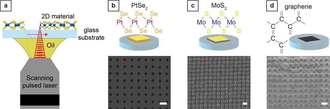 |
| Nanopatterning of 2D supplies utilizing a two-photon 3D printer. (a) 3D schematic of the laser writing strategy. The 2D materials is both grown or transferred on the entrance aspect of a skinny glass coverslip. (b), (c), and (d) current nanohole arrays in platinum diselenide (PtSe2), molybdenum disulfide (MoS2), and graphene, respectively. Scale bar, 1 μm for PtSe2, 500 nm for MoS2, and 300 nm for graphene. (Picture: Graphene Flagship)
|
|
The following step is to research the compatibility of this methodology with suspended 2D materials membranes and change the glass substrate with different purposeful ones.
|
|
This mission was executed throughout the Graphene Flagship and the Graphene Flagship Partnering Undertaking FLAG‐ERA JTC 2019 2D‐NEMS, which is affiliated with the Sensors Work Package deal of the Graphene Flagship.
|
