| Aug 24, 2023 |
|
(Nanowerk Information) Utilizing DNA applied sciences to create a brand new era of tiny electronics parts at low manufacturing prices: that is the primary aim of the European-funded undertaking 3D-BRICKS, coordinated by Istituto Italiano di Tecnologia (IIT-Italian Institute of Expertise) in Genoa (Italy), and involving an interdisciplinary crew of prime researchers from Italy, Spain, Germany, Belgium, and Switzerland.
|
|
The undertaking, which has been based by the European Union beneath the Horizon EU framework program with 3.7 million euro for the following 3 years, is coordinated by Denis Garoli and Remo Proietti Zaccaria, researchers on the IIT in Genoa.
|
|
The present semiconductors and nanoelectronics applied sciences are primarily based on steel–oxide–semiconductor gadgets, whose efficiency is near its finish. Various applied sciences, which could have the ability to carry out higher by way of computing energy and vitality effectivity, haven’t but been recognized.
|
|
Researchers of the 3D-BRICKS undertaking need to concentrate on the usage of carbon nanotubes – probably the most promising candidates due to their nano dimensions – along with DNA applied sciences, to acquire nano-transistors with unprecedented measurement, performances, and low manufacturing prices.
|
|
The present fabrication strategy of high-performance carbon nanotube-based transistors is extraordinarily difficult. The 3D-BRICKS undertaking will introduce a organic method, within the sense that researchers need to deploy the power of DNA to naturally create 2D and 3D geometries, by utilizing 3D DNA-nanostructures as template for transistors, digital logics and reminiscence.
|
|
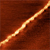
Carbon nanotubes will likely be used as a “brick” in a position to prepare in a self-assembling supplies, equivalent to metals and semiconductors, at nanometer dimension.
|
|
Using nanomaterials anchored alongside the DNA provider allows to scale back considerably the complexity and the time price of the fabrication, with a spatial decision near the diameter of double strand DNA (ca. 2 nanometers). As soon as a single layer of fabric is realized, the 3D-BRICKS undertaking will then carry the biofabrication of 3D-Carbon Nanotubes transistors on a brand new degree by taking part in with the third dimension, the place a number of layers of digital logics built-in in the identical construction.
|
|
This novel method will permit to understand nano transistors in a extra compact and environment friendly approach, paving the way in which for science tech industries of the longer term.
|
|
Along with IIT, the 3D-BRICKS consortium consists by: College of Fribourg (Switzerland), Universitaet Leipzig (Germany), Universitaet Hamburg (Germany), Universiteit Antwerpen (Belgium), Karlsruher Institut Fuer Technologie (Germany), KERR S.R.L. (Italy), Fundacio Institut Catala De Nanociencia y Nanotecnologia (Spain), CNT Innovation (Belgium).
|
