| Sep 04, 2023 |
|
(Nanowerk Information) A revolution in know-how is on the horizon, and it’s poised to alter the units that we use. Underneath the distinguished management of Professor LEE Younger Hee, a group of visionary researchers from the Middle for Built-in Nanostructure Physics inside the Institute for Fundamental Science (IBS), South Korea, has unveiled a brand new discovery that may enormously enhance the fabrication of field-effect transistors (FET).
|
|
The analysis has been revealed in Nature Nanotechnology (“Low Ohmic contact resistance and excessive on/off ratio in transition metallic dichalcogenides field-effect transistors by way of residue-free switch”).
|
|
A high-performance field-effect transistor (FET) is a necessary constructing block for next-generation beyond-silicon-based semiconductor applied sciences. Present three-dimensional silicon know-how suffers from degradation of FET performances when the machine is miniaturized previous sub-3-nm scales. To beat this restrict, researchers have studied one-atom thick (~0.7 nm) two-dimensional (2D) transition metallic dichalcogenides (TMDs) as a really perfect FET platform during the last decade. However, their sensible functions are restricted because of the incapability to display integration on the wafer-scale.
|
|
A significant downside is the residues that happen throughout fabrication. Historically, polymethyl methacrylate (PMMA) is used as a supporting holder for machine switch. This materials is infamous for leaving insulating residues on TMD surfaces, which regularly generates mechanical harm to the delicate TMD sheet throughout switch. As a substitute for PMMA, a number of different polymers resembling polydimethylsiloxane (PDMS), polyvinyl alcohol (PVA), polystyrene (PS), polycarbonate (PC), ethylene vinyl acetate (EVA), polyvinylpyrrolidone (PVP) and natural molecules together with paraffin, cellulose acetate, naphthalene have all been proposed as a supporting holder. However, residues and mechanical damages are inevitably launched throughout switch, which ends up in degradation of FET performances.
|
|
The IBS researchers addressed this downside and have made an intriguing breakthrough by efficiently harnessing polypropylene carbonate (PPC) for residue-free moist switch. Utilizing PPC not solely eradicated residue but additionally allowed for the manufacturing of wafer-scale TMD utilizing chemical vapor deposition. Earlier makes an attempt at manufacturing large-scale TMDs typically resulted in wrinkles, which happen throughout the switch course of. The weak binding affinity between the PPC and the TMD not solely eradicated residues however wrinkles as nicely.
|
|
Mr. Ashok MONDAL, the primary creator of the examine mentioned, “The PPC switch technique we selected permits us to manufacture centimeter-scale TMDs. Beforehand, TMD was restricted to being produced utilizing a stamping technique, which generates flakes which are solely 30-40 µm in measurement.”
|
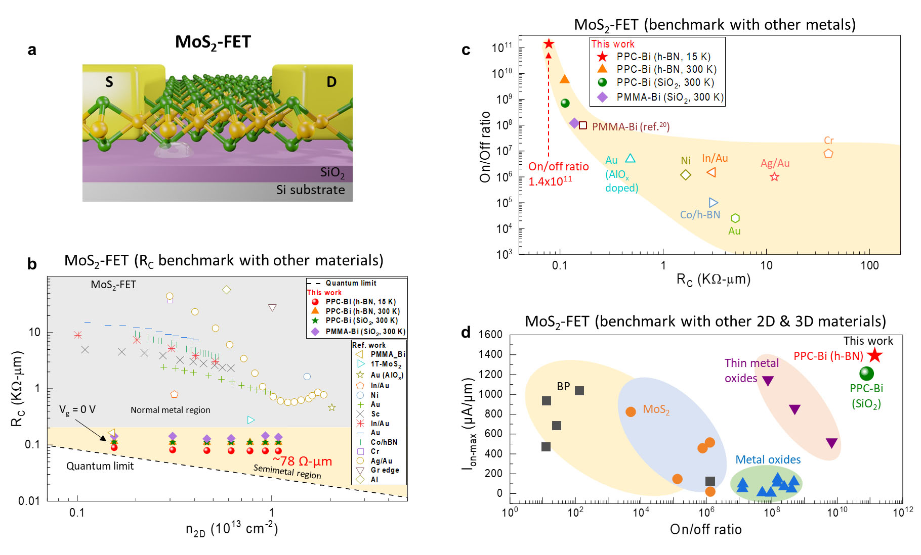 |
| Benchmark of ultra-clean large-area monolayer MoS2-FET. (a) MoS2 FET machine schematic. (b) Benchmark of RC vs. n2D in MoS2 FET utilizing totally different metallic contacts for varied semiconductor applied sciences. (c) Benchmark of on/off ratio vs. RC in MoS2 FET in comparison with totally different metallic contacts utilized in semiconductor applied sciences. (d) Benchmark of the utmost on-current (Ion-max) vs. on/off ratio of the MoS2 FET for PPC-Bi contact in comparison with stories described within the literature.
|
|
The researchers constructed a FET machine utilizing a semimetal Bi contact electrode with a monolayer of MoS2, which was transferred by the PPC technique. Lower than 0.08% of PPC residue was discovered to stay on the MoS2 layer. Because of the dearth of interfacial residues, the machine was discovered to have an ohmic contact resistance of RC ~78 Ω-µm, which is near the quantum restrict. An ultrahigh present on/off ratio of ~1011 at 15 Ok and a excessive on-current of ~1.4 mA/µm have been additionally achieved utilizing the h-BN substrate.
|
|
This discovering was the primary on the planet that demonstrated wafer-scale manufacturing and switch of CVD-grown TMD. The state-of-the-art FET machine produced on this method was discovered to have electrical properties that far exceed that of beforehand reported values. It’s believed that this know-how might be simply carried out utilizing the presently obtainable built-in circuit manufacturing know-how.
|
|
Dr. Chandan BISWAS, the co-corresponding creator of the examine mentioned, “It’s hoped that our success within the residue-free PPC switch method will encourage different researchers to develop additional enhancements in varied TMD units sooner or later.”
|
