| Jul 13, 2023 |
|
(Nanowerk Information) The Huge Knowledge revolution has strained the capabilities of state-of-the-art digital {hardware}, difficult engineers to rethink nearly each side of the microchip. With ever extra huge information units to retailer, search and analyze at growing ranges of complexity, these units should develop into smaller, sooner and extra power environment friendly to maintain up with the tempo of knowledge innovation.
|
|
Ferroelectric subject impact transistors (FE-FETs) are among the many most intriguing solutions to this problem. Like conventional silicon-based transistors, FE-FETs are switches, turning on and off at unimaginable pace to speak the 1s and 0s computer systems use to carry out their operations.
|
|
However FE-FETs have a further operate that standard transistors don’t: their ferroelectric properties permit them to carry on to electrical cost.
|
|
This property permits them to function non-volatile reminiscence units in addition to computing units. In a position to each retailer and course of information, FE-FETs are the topic of a variety of analysis and improvement tasks. A profitable FE-FET design would dramatically undercut the dimensions and power utilization thresholds of conventional units, in addition to enhance pace.
|
|
Researchers on the College of Pennsylvania College of Engineering and Utilized Science have launched a brand new FE-FET design that demonstrates record-breaking performances in each computing and reminiscence.
|
 |
| Researchers on the College of Pennsylvania College of Engineering and Utilized Science have launched a brand new FE-FET design that demonstrates record-breaking performances in each computing and reminiscence. (Picture: Penn Engineering)
|
|
A latest research printed in Nature Nanotechnology (“Scalable CMOS back-end-of-line-compatible AlScN/two-dimensional channel ferroelectric field-effect transistors”) led by Deep Jariwala, Affiliate Professor within the Division of Electrical and Techniques Engineering (ESE), and Kwan-Ho Kim, a Ph.D. candidate in his lab, debuted the design. They collaborated with fellow Penn Engineering college members Troy Olsson, additionally Affiliate Professor in ESE, and Eric Stach, Robert D. Bent Professor of Engineering within the Division of Supplies Science and Engineering (MSE) and Director of the Laboratory for Analysis on the Construction of Matter (LRSM).
|
|
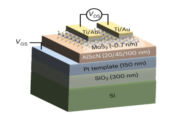
The transistor layers a two-dimensional semiconductor known as molybdenum disulfide (MoS2) on high of a ferroelectric materials known as aluminum scandium nitride (AlScN), demonstrating for the primary time that these two supplies could be successfully mixed to create transistors at scales engaging to industrial manufacturing.
|
|
“As a result of now we have made these units combining a ferroelectric insulator materials with a 2D semiconductor, each are very power environment friendly,” says Jariwala. “You need to use them for computing in addition to reminiscence — interchangeably and with excessive effectivity.”
|
|
The Penn Engineering group’s machine is notable for its unprecedented thinness, permitting for every particular person machine to function with a minimal quantity of floor space. As well as, the tiny units could be manufactured in giant arrays scalable to industrial platforms.
|
|
“With our semiconductor, MoS2, at a mere 0.7 nanometers, we weren’t positive it might survive the quantity of cost that our ferroelectric materials, AlScN, would inject into it,” says Kim. “To our shock, not solely did each of them survive, however the quantity of present this permits the semiconductor to hold was additionally record-breaking.”
|
|
The extra present a tool can carry, the sooner it may possibly function for computing functions. The decrease the resistance, the sooner the entry pace for reminiscence.
|
|
This MoS2 and AlScN mixture is a real breakthrough in transistor expertise. Different analysis groups’ FE-FETs have been constantly stymied by a lack of ferroelectric properties as units miniaturize to strategy industry-appropriate scales.
|
|
Till this research, miniaturizing FE-FETs has resulted in extreme shrinking of the “reminiscence window.” Because of this as engineers cut back the dimensions of the transistor design, the machine develops an unreliable reminiscence, mistaking 1s for 0s and vice versa, compromising its total efficiency.
|
|
The Jariwala lab and collaborators achieved a design that retains the reminiscence window giant with impressively small machine dimensions. With AlScN at 20 nanometers, and MoS2 at 0.7 nanometers, the FE-FET dependably shops information for fast entry.
|
|
“The important thing,” says Olsson, “is our ferroelectric materials, AlScN. Not like many ferroelectric supplies, it maintains its distinctive properties even when very skinny. In a latest paper from my group, we confirmed that it may possibly we will retain its distinctive ferroelectric properties at even smaller thicknesses: 5 nanometers.”
|
|
The Penn Engineering group’s subsequent steps are centered on this additional miniaturization to provide units that function with voltages low sufficient to be appropriate with modern shopper machine manufacturing.
|
|
“Our FE-FETs are extremely promising,” says Jariwala. “With additional improvement, these versatile units might have a spot in nearly any expertise you may consider, particularly these which might be AI-enabled and eat, generate or course of huge quantities of knowledge — from sensing to communications and extra.”
|
