| Sep 18, 2023 |
|
(Nanowerk Information) A analysis staff, led by Professor Joonki Suh within the Division of Supplies Science and Engineering and the Graduate Faculty of Semiconductor Supplies and Units Engineering at UNIST, has made a major breakthrough in skinny movie deposition expertise. By using an modern atomic layer deposition (ALD) course of, Professor Search engine marketing efficiently achieved common association of tellurium (Te) atoms at low temperatures as little as 50 levels Celsius.
|
|
The ALD technique is a cutting-edge skinny movie course of that allows exact stacking of semiconductor supplies on the atomic layer degree on three-dimensional buildings—even at low course of temperatures. Nevertheless, conventional software to next-generation semiconductors requires excessive processing temperatures above 250 levels Celsius and extra warmth therapy exceeding 450 levels Celsius.
|
|
On this groundbreaking analysis (ACS Nano, “Atomic Layer Deposition Path to Scalable, Digital-Grade van der Waals Te Skinny Movies”), the UNIST staff utilized ALD to monoelemental van der Waals tellurium—a cloth below in depth investigation for its potential purposes in digital units and thermoelectric supplies. Remarkably, they efficiently fabricated high-quality Te skinny movies with none post-deposition warmth therapy at an unprecedentedly low temperature of solely 50 levels Celsius. The ensuing movies exhibited distinctive uniformity with exactly managed thickness all the way down to nanometers scale—attaining good atom association with one out of each billion atoms.
|
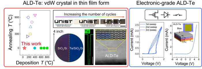 |
| Scalability, controllability, and homogeneity of atomic layer deposited tellurium (ALD-Te). (Picture: UNIST)
|
|
To boost reactivity at decrease temperatures, the analysis staff employed two precursors with acid-base properties. Moreover, they launched co-reactants to enhance floor reactions and stability whereas adopting a repeating dosing method by injecting precursors in shorter intervals. These methods enabled the manufacturing of dense and steady Te skinny movies in comparison with standard strategies that usually resulted in porous or discontinuous grain depositions.
|
|
The developed manufacturing course of allowed for wafer-scale development on whole 4-inch (100mm) wafers, offering exact atomic layer-level thickness management and uniform deposition. Moreover, the Te skinny movies demonstrated compatibility with vertical three-dimensional buildings—a vital requirement for prime gadget integration. This breakthrough holds vital potential for numerous digital units equivalent to transistors, rectifiers, and choice parts.
|
|
“This analysis fulfills all of the important standards of low-temperature, large-area, and high-quality synthesis in semiconductor deposition processes,” acknowledged Professor Suh.
|
