
Welcome again, all! At this time we’re gonna proceed on our PCB design journey with surface-mount expertise, an method that’s usually more economical, environment friendly, and house conserving than utilizing conventional through-hole parts. For those who haven’t already, you should definitely try the primary EasyEDA weblog publish to get set-up and we’ll dive proper in!
Putting Parts in our Schematic
Okay, so, identical to final time we’re gonna open up the EasyEDA designer and create a brand new undertaking (I didn’t separate mine at first however go forward and create a brand new folder relatively than embody it with our final board design) and add our parts. I’ll present the LCSC product codes that I used simply to get us shifting and good to go, however positively try the LCSC web site and get accustomed to discovering what you want.
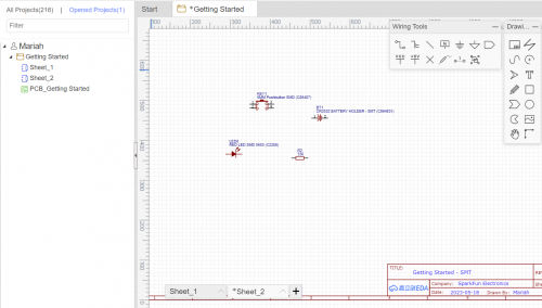
- Battery: C964831
- Button: C86487
- Resistor: C101329
- LED: C2286
Connecting our Circuit
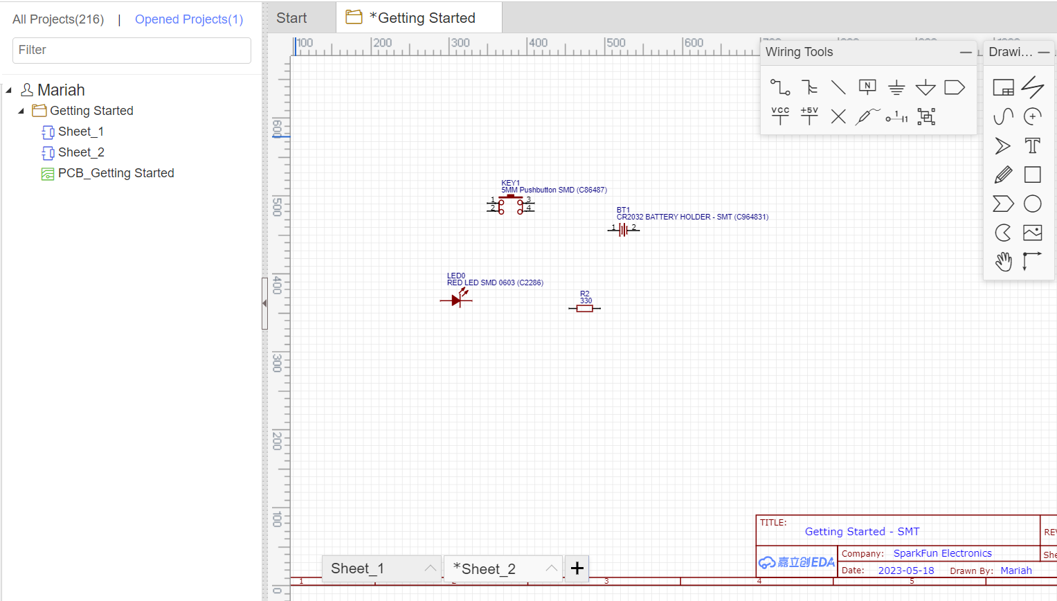
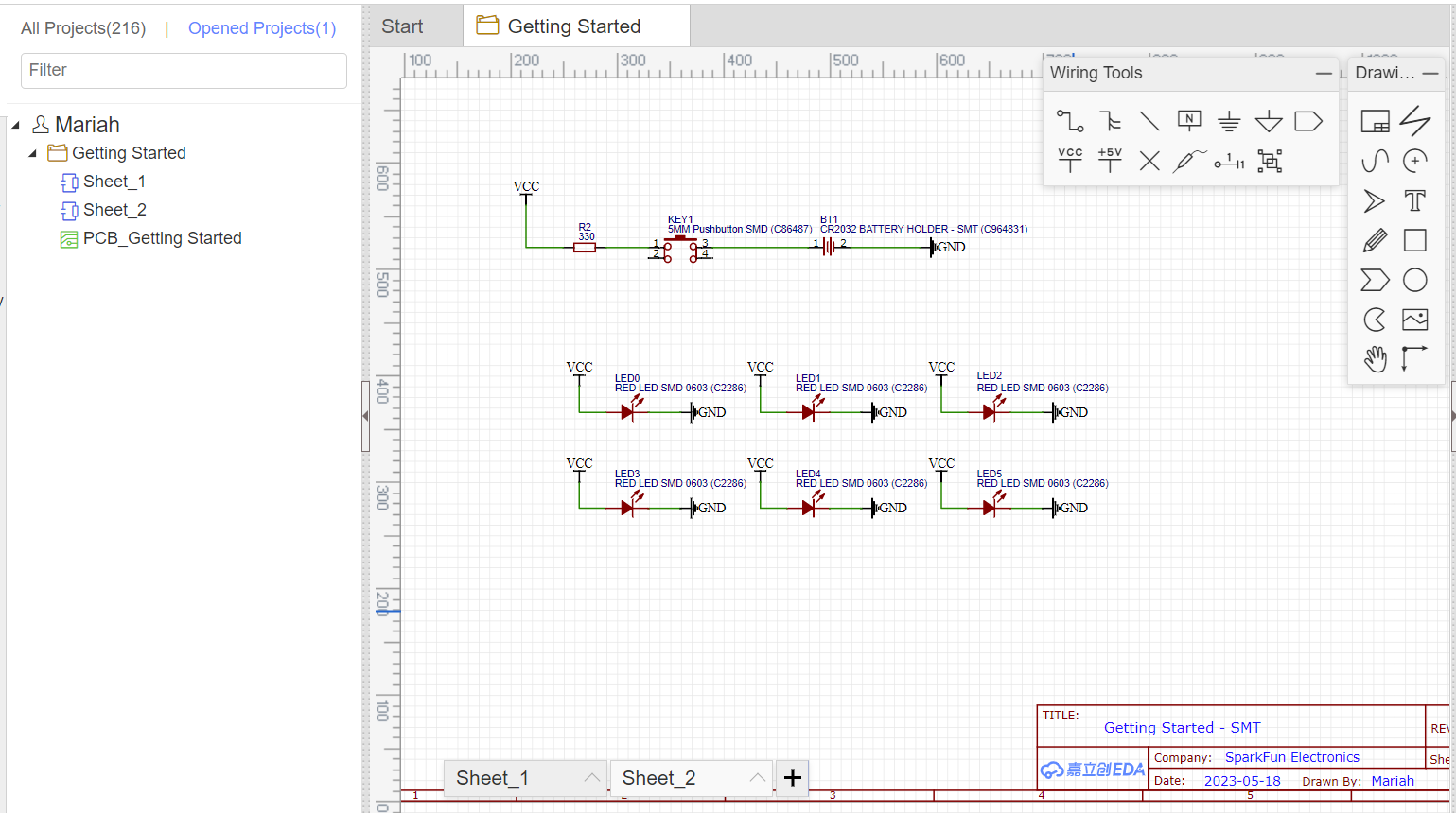
Alright, so now we’ve bought our pals in right here and you might be questioning why they don’t look any completely different from our through-hole components from earlier than; mainly our schematic diagrams don’t change a lot since we’re extra apprehensive about the kind of half on this stage. As soon as we get to the PCB portion you’ll discover the distinction! Let’s go forward and format and join our parts:
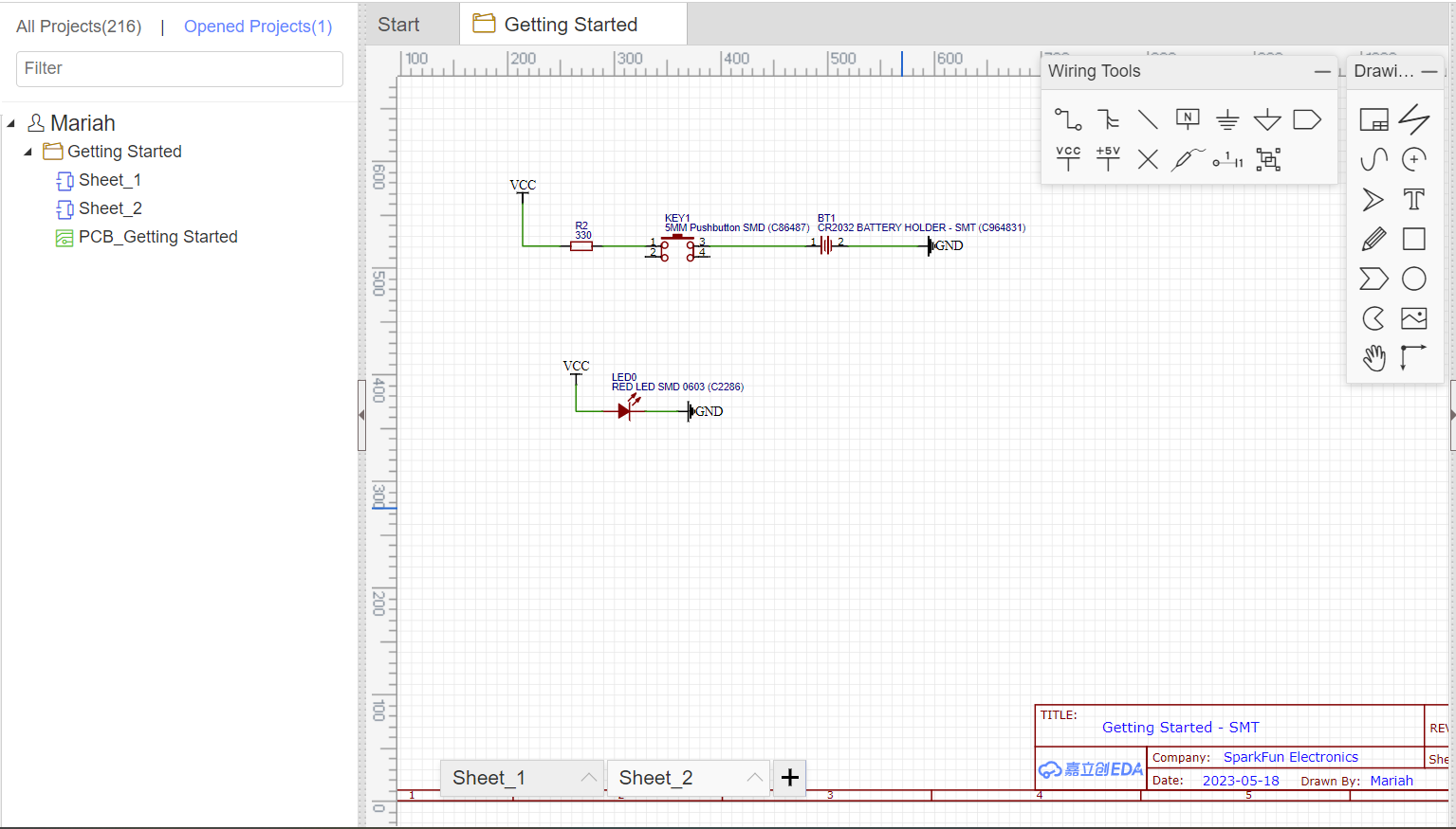
So we’ve related issues a bit in another way from earlier than and it’ll turn into clear as to why after we begin making traces on our board; for now, I’m gonna throw in some extra LEDs for funsies, principally as a result of the SMT LEDs are very small (we’re utilizing 0603 components, which is 60 mils by 30 mils, and one mil is 1/a thousandth of an inch, or 0.001 inches) and I need to take up some extra space on our board.
Producing the PCB
Now for the enjoyable half! Let’s go as much as the design tab and convert our schematic to a PCB (keep in mind that we’re pleased with not checking nets or messing with any of the default settings that pop up right here).
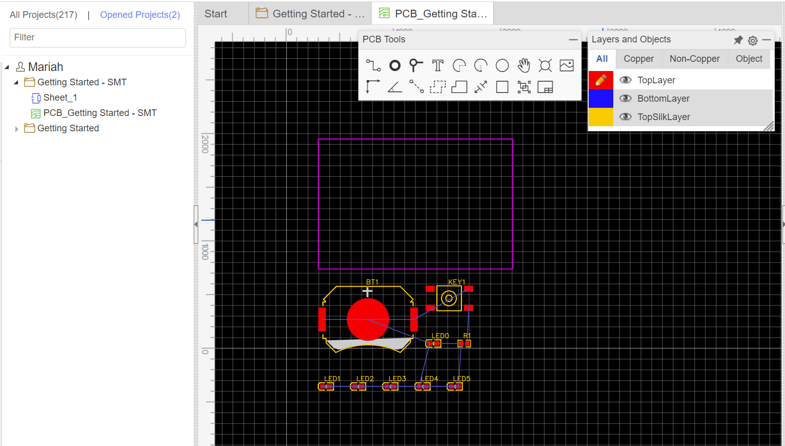
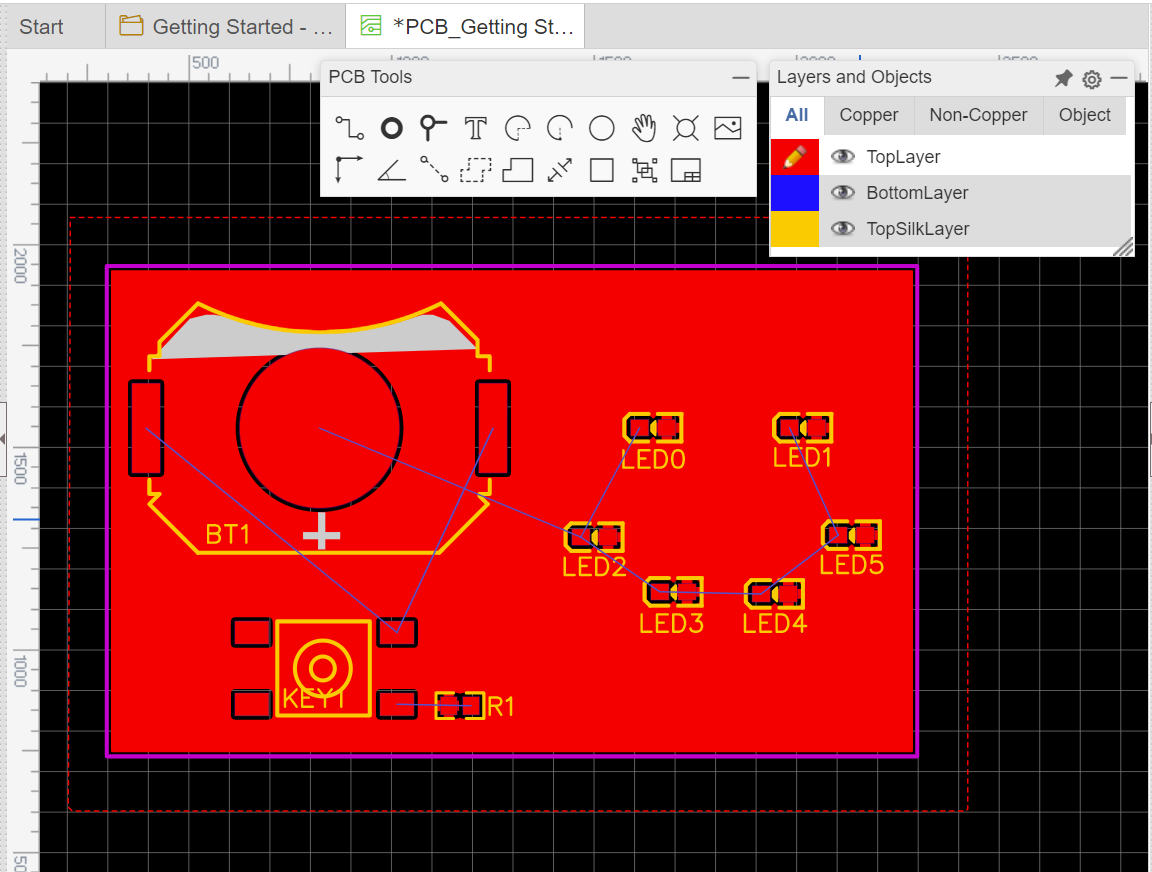
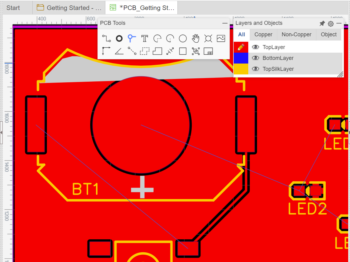
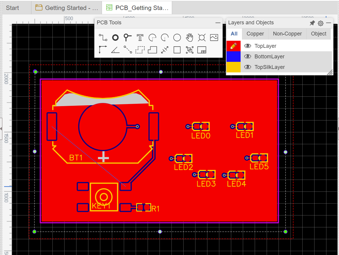
These are surface-mount parts! See what I imply concerning the teeny-tiny LEDs? Let’s lay out our parts how we’d like them; one factor to notice is that the battery has a curved facet and a straight facet. The curved facet is the place the CR2032 battery will slot in, so we need to take that into consideration with how we orient issues. I’m going to have it slot in from the highest as a result of I would like the button to be beneath the battery, so I rotated that half 180 levels so the button wouldn’t intervene with it. I additionally organized my LEDs in a smiley face just because I can!
I did have to increase the board define simply a bit to get the look that I wished, which you are able to do by choosing the facet you need to transfer and both dragging it with the mouse or utilizing the arrow keys to maneuver it in increments of your snap measurement. I additionally went forward and cleaned up my silk layer as properly at this level in order that the labels have been the place I wished them.
Making a VCC Airplane
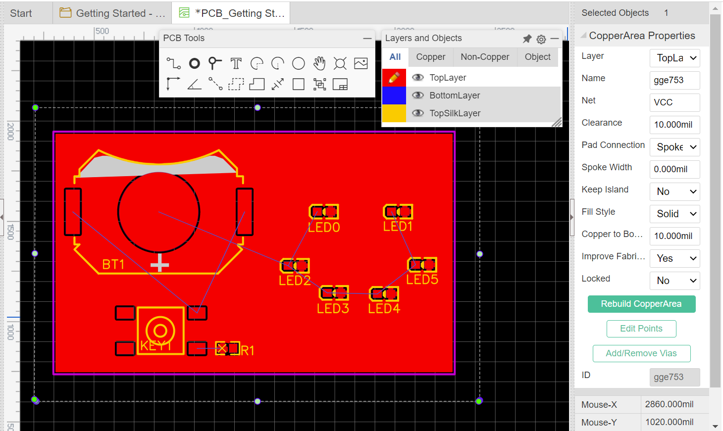
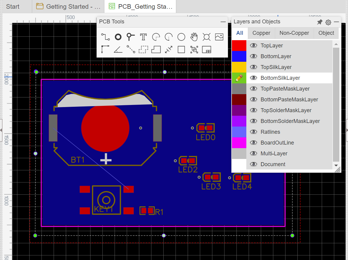
Now right here’s the place issues get actually fancy; we’re going to create one thing known as a copper space. Basically what this does is create a whole layer of copper throughout the whole board; then we will label that space as a connection we intend to make, which permits us to make that connection at any level on the board. It’ll make extra sense as soon as it’s there, I promise! So let’s choose the device that appears like a dashed define of a Tetris piece:
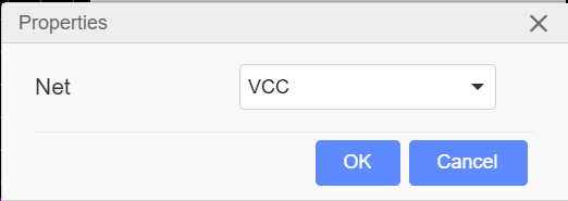
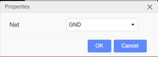
As soon as you choose the device, a ‘Properties’ pop-up will ask what you’d just like the ‘Internet’ for this layer to be (a internet is a designation that may inform this system what a part of our circuit we would like it to hook up with). We’re going to have this be a VCC airplane:
Now, with that device energetic, we’re going to click on as soon as in all 4 corners outdoors of our board define and proper click on to exit and construct out the layer, like so:
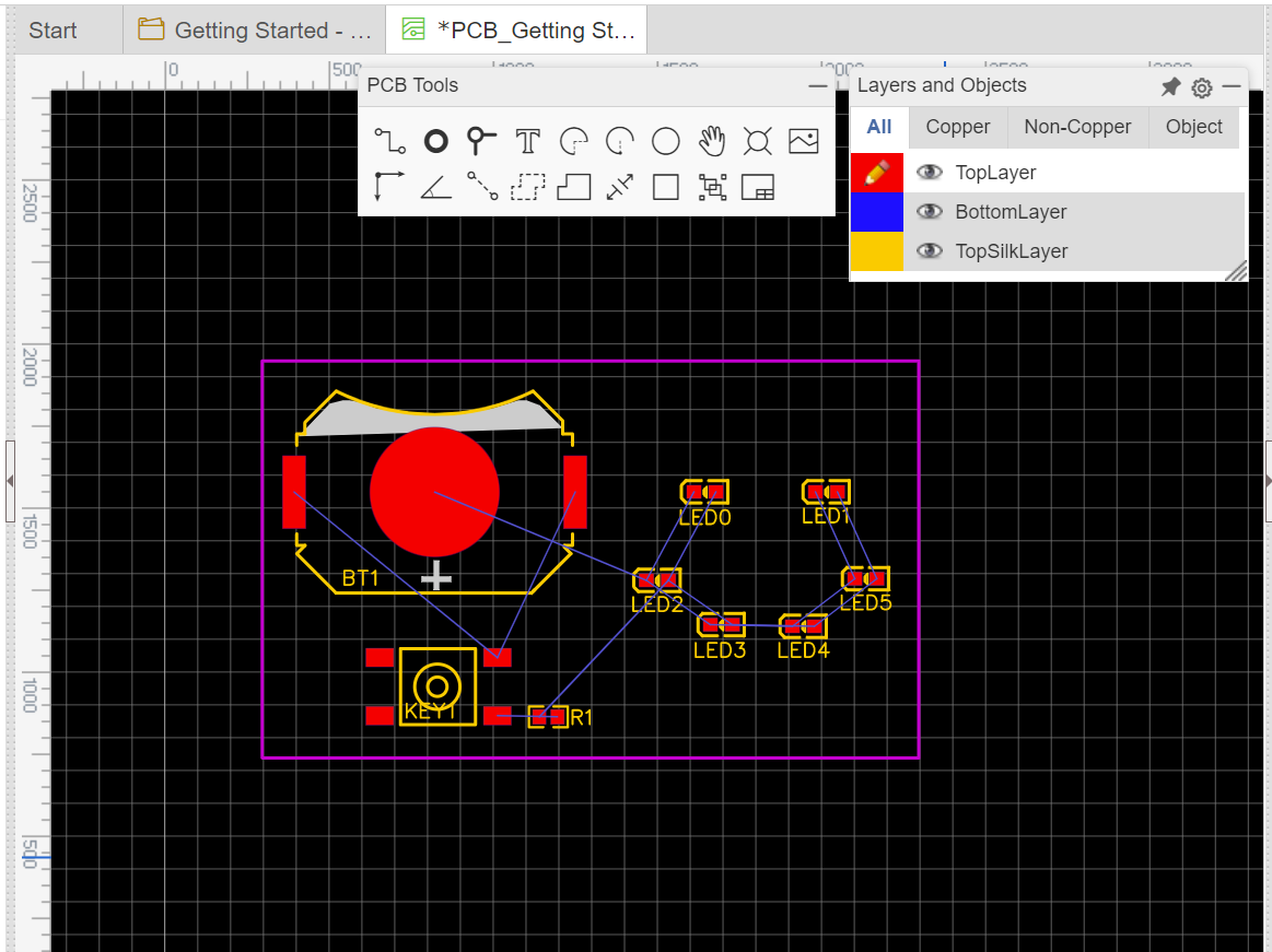
With the copper space crammed in, we will see higher what it’s doing right here: you’ll discover that something that isn’t related to a VCC flag on our schematic is remoted from the copper layer and every little thing that’s has a tab-like look on the pad permitting it to make contact with the airplane! This actually is useful with difficult boards and reduces the variety of potential crossovers with our traces.
how I had issues laid out and my remaining rat’s nest strains, I spotted it’d make far more sense for me to flip my resistor spherical to make the hint extra direct. One factor to notice is that the copper layer doesn’t routinely replace, so flipping my resistor now implies that the pads have modified locations and the connections are incorrect (you’ll discover the little yellow ‘X’ on one facet letting me know that there’s a connection made that I didn’t need). However to not fear! There’s a simple repair to this: click on on the dashed define of our copper space that we drew earlier. On the proper facet of the display screen, you’ll see a button that claims “Rebuild Copper Space”; that may regenerate the layer and repair our concern!
Making Traces on the Energy Airplane
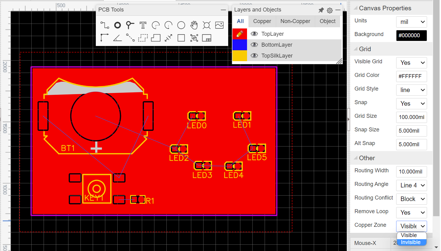
Our VCC is all set, however we nonetheless have a number of connections left! Let’s take a look at hooking up our battery, button, and resistor. We may simply join them with the copper layer energetic, however it may be actually onerous to see the place we’re going within the mess of vivid crimson. On the proper facet of the display screen, you’ll see an possibility labeled ‘Copper Zone’ (this exhibits up with the copper space DEselected, so simply click on off to the facet and it ought to pop up); this menu has a drop down choice to make the copper layer invisible, which we’ll go forward and choose so we will see what we’re doing.
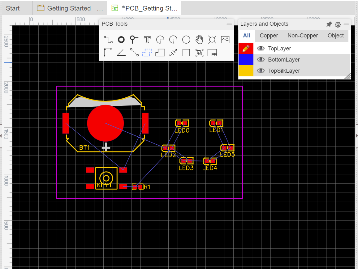
With that executed now we will create our traces from the battery, to the button, to the resistor. You’ll discover that there are two rat’s nest strains coming from the battery to the button; that is simply because of the nature of this half the place the 2 metallic tabs on both facet are in touch with the constructive facet of the battery. You possibly can join each to the button, or one to the opposite after which to the button, or only one to the button and ignore the opposite. Completely as much as you, I simply related one facet and let the opposite be.
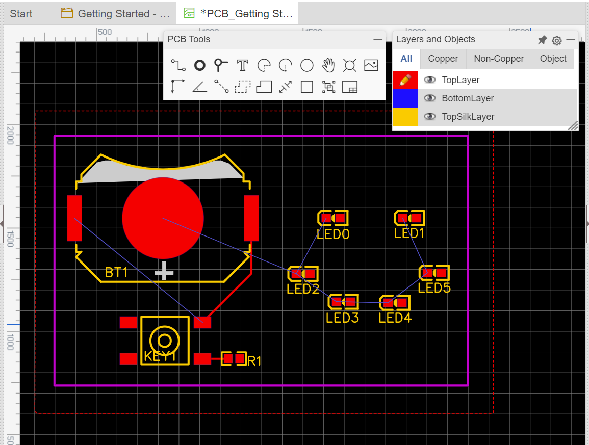
Now that these are good to go, we will rebuild our copper space and switch it again on:

You possibly can even see right here how our traces are additionally remoted from the copper space! I believe it has a very neat look.
Making a GND Airplane and Utilizing Vias
Okay! Now all that’s left is to get our GND connections in place and we’re good to go. Let’s make our backside layer energetic from our ‘Layers and Objects’ menu, and choose the copper space device once more. This time, we’re going to set our internet to ‘GND’ and do the identical course of as earlier than:
Now, till we now have an element connecting to the layer, it received’t populate beneath, however I promise it’s there! So, how can we join one thing on one layer of the board to the again when it doesn’t poke via the board? Utilizing a brilliant helpful device known as a ‘By way of’! Within the toolbar, it’s the proper angle with the small circle within the nook:
We’re going to put our through subsequent to this large circle in the course of our battery; what this enables us to do is run a hint from that pad to the through, which can bore via the board and join it to the GND airplane we put beneath!
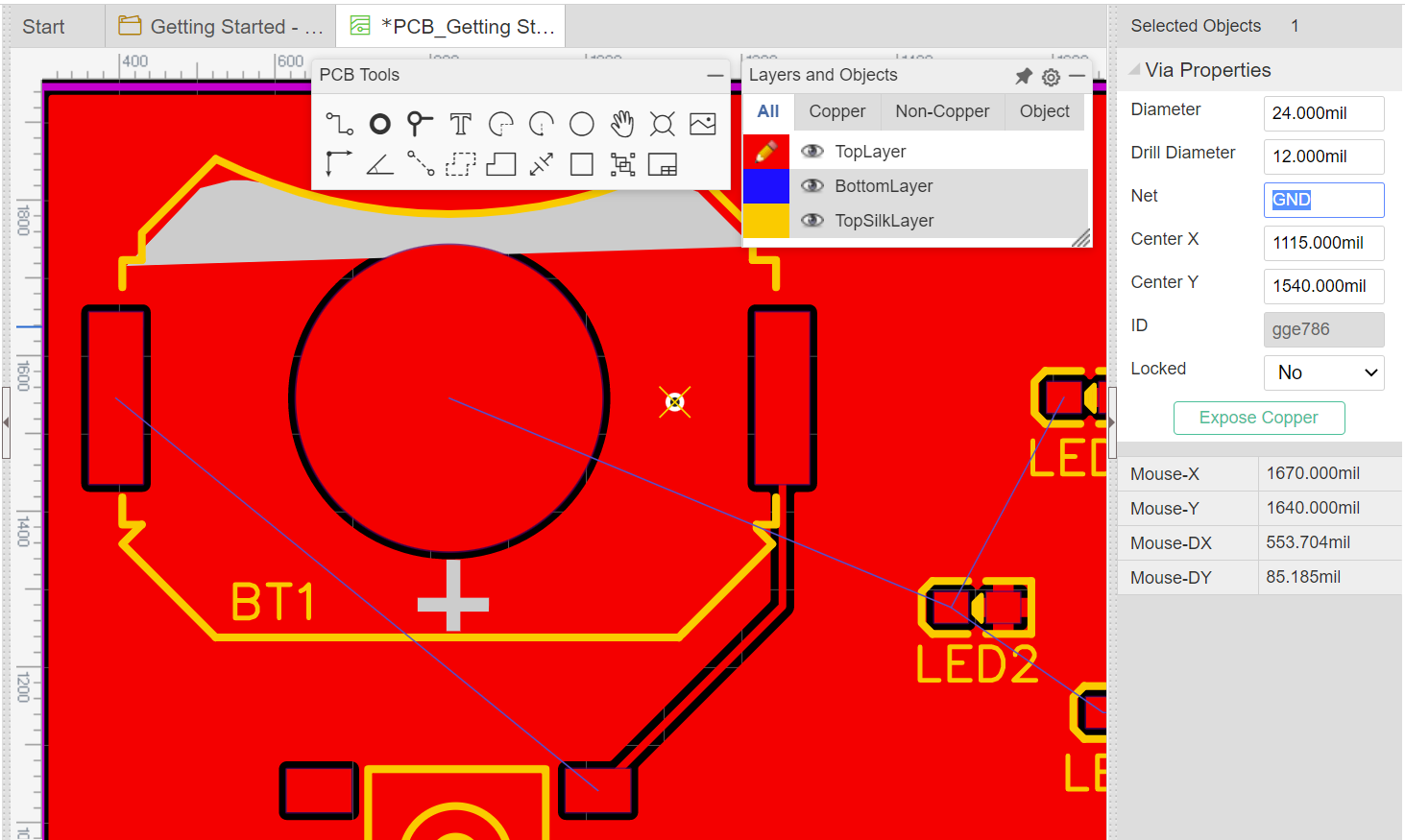
As soon as it’s positioned, choose it yet one more time and alter the ‘Internet’ on the proper hand facet to say ‘GND’; it will let the designer know that we would like the through to hook up with our GND airplane on the again, and permit us to run a hint between it and the battery pad.
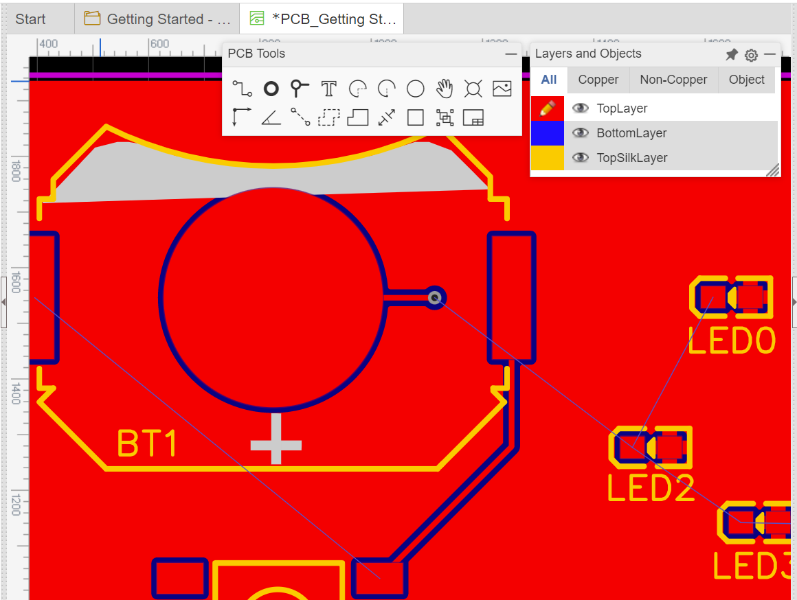
Right here’s the place we will see the underside layer airplane as that blue space that’s proven up. Informed ya it was there! Now all that’s left is to put vias by our LEDs and get them related to GND as properly (fortunately we solely have to call our vias as soon as and it’ll hold the final internet entered energetic). Bear in mind to rebuild BOTH of your copper areas when you’ve made all of the connections!
Ending Touches
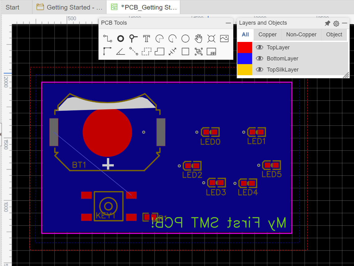
And that’s all there may be to it! Let’s slap a label on this unhealthy boy and name it good! This time, we’re going to pick ‘BottomSilkLayer’ from the ‘Layers and Objects’ menu.
Then, like final time, we’ll choose our textual content device and write what we would like our board to be known as (it’ll seem backwards because it’s on the again of our board)!
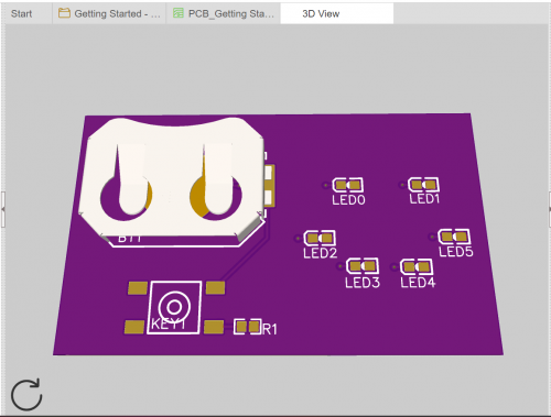
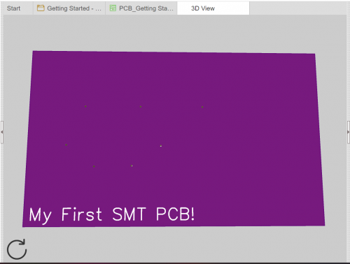
Achieved! Now let’s try the 3D view! What’s tremendous cool is that some parts have a 3D mannequin so we will see what it would truly appear to be with the half on the board. I went with purple as the colour this time for funsies.
What’s subsequent?
Thanks guys for becoming a member of in on getting began with SMT PCB design! As all the time, let me know in case you have any questions or need to see something specifically and I’ll do my finest to make it occur. Come again subsequent time after we’ll discover a little bit of the extra inventive elements of designing your personal PCBs!