| Jul 26, 2023 |
|
(Nanowerk Information) Photonic methods are rapidly gaining traction in lots of rising functions, together with optical communications, lidar sensing, and medical imaging. Nonetheless, the widespread adoption of photonics in future engineering options hinges on the price of manufacturing photodetectors, which, in flip, largely will depend on the sort of semiconductor utilized for the aim.
|
|
Historically, silicon (Si) has been probably the most prevalent semiconductor within the electronics trade, a lot in order that many of the trade has matured round this materials. Sadly, Si has a comparatively weak gentle absorption coefficient within the near-infrared (NIR) spectrum in comparison with these of different semiconductors reminiscent of gallium arsenide (GaAs). Due to this, GaAs and associated alloys thrive in photonic functions, however are incompatible with the normal complementary metal-oxide-semiconductor (CMOS) processes used within the manufacturing of most electronics. This results in a drastic improve of their manufacturing prices.
|
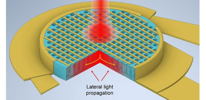 |
| Photon-trapping micro- and nano-sized holes in silicon (Si) make usually incident gentle bend by virtually 90°, making it propagate laterally alongside the aircraft and main consequently to elevated gentle absorption within the NIR band. (Picture: Qarony, Mayet, et al., doi 10.1117/1.APN.2.5.056001)
|
|
To deal with this downside, a analysis group from UC Davis in California is pioneering a brand new technique to vastly increase the sunshine absorption of skinny Si movies. Of their newest paper revealed in Superior Photonics Nexus (“Attaining greater photoabsorption than group III-V semiconductors in ultrafast skinny silicon photodetectors with built-in photon-trapping floor constructions”), they current the primary experimental demonstration of Si-based photodetectors with light-trapping micro- and nano-surface constructions, reaching unprecedented efficiency positive factors that rival that of GaAs and different group III-V semiconductors.
|
|
The proposed photodetectors include a micrometer-thick cylindrical Si slab positioned over an insulating substrate, with metallic “fingers” extending from the contact metals atop the slab in an interdigitated trend. Importantly, the majority Si is full of round holes organized in a periodic sample that act as photon-trapping websites. The general construction of the system causes usually incident gentle to bend by virtually 90° upon hitting the floor, making it journey laterally alongside the Si aircraft. These laterally propagating modes improve the propagation size of sunshine and successfully gradual it down, resulting in extra gentle–matter interplay and a consequent improve in absorption.
|
|
The researchers moreover carried out optical simulations and theoretical analyses to higher perceive the results of the photon-trapping constructions, and carried out a number of experiments evaluating photodetectors with and with out them. They discovered that photon trapping led to a outstanding improve within the absorption effectivity over a large band within the NIR spectrum, staying above 68 p.c and peaking at 86 p.c.
|
|
Notably, the noticed absorption coefficient of the photon-trapping photodetector was a number of occasions greater than that of plain Si and exceeded that of GaAs within the NIR band. Moreover, though the proposed design was for a 1-μm-thick Si slab, simulations of 30- and 100-nm Si skinny movies appropriate with CMOS electronics confirmed a equally enhanced efficiency.
|
|
General, the findings of this examine exhibit a promising technique to spice up the efficiency of Si-based photodetectors for rising photonics functions. By reaching excessive absorption even in ultrathin Si layers, the parasitic capacitance of the circuit will be saved low, which is essential in high-speed methods. Furthermore, the proposed method is appropriate with trendy CMOS manufacturing processes, and might thus doubtlessly revolutionize the best way during which optoelectronics are built-in into standard circuits. In flip, this might pave the best way for reasonably priced ultrafast laptop networks and substantial leaps in imaging expertise.
|
