
Excessive-speed PCB design consists of a number of steps. Design re-spin is just not solely cost-sensitive but in addition time-consuming. So, one ought to comply with correct design guidelines early within the design cycle to have the PCB working on the very first try
Printed circuit board (PCB) is an important a part of all digital items, ranging from digital toys, distant controls, and cellphones to advanced digital circuits in telecom tools, airplanes, spacecraft, and medical gadgets. With speedy developments within the electronics business and the miniaturization of elements, PCB design has gone by way of a speedy evolution in the previous couple of many years.
From PCBs of some layers and largely through-hole elements, PCBs these days have tens of layers, fine-pitch elements, and a combination of through-hole and floor mount elements. Fashionable advanced designs at instances require versatile PCBs and embedded elements.
PCBs which might be designed for high-speed indicators (greater than 1Gbps) want particular consideration throughout design as sign high quality (rise/fall time, crosstalk, attenuation, and so on) performs a vital function in dependable operation. Excessive-speed PCB design consists of a number of steps. Design re-spin is just not solely cost-sensitive but in addition time-consuming.
Excessive-speed PCB Design Movement
It’s higher to comply with correct design guidelines early within the design cycle to have the PCB working on the very first try. Fig. 1 exhibits the most important steps concerned in a high-speed PCB design. Let’s undergo the most important steps one after the other.

Schematic design: The design begins with a schematic drawing. There are lots of open sources in addition to licensed software program out there for schematic design. However whereas designing a fancy PCB design, it’s higher to go for reputed licensed variations as they provide higher integration with the format, helpful options for faster designs, and higher constraint administration.
Throughout schematic drawing, the main target ought to be on the performance of the circuit and the choice of elements. Throughout the choice of the elements, the specs to search for are dimension, energy dealing with capability, footprint, stray inductances and capacitances related to that element, working temperature vary, and moisture sensitivity stage (MSL).
Though the techniques on chips (SoCs), discipline programmable gate arrays (FPGAs), and application-specific built-in circuits (ASICs) largely are available ball grid array (BGA) packages, some ICs can be found in a number of packages like SSOP, TSSOP, SO, and so on. The important thing issues to pick a package deal are value, temperature vary, warmth dissipation, actual property on the PCB, and lead time.
After the components are finalized, symbols and footprints equivalent to these components must be created to proceed with the schematic. You will need to evaluation the design fastidiously to verify the specified performance and any errors like improper connection, unconnected nets, incorrect package deal choice, and so on.
Part footprints additionally must be checked fastidiously for his or her mechanical dimensions, pin sequences, and so on. Solely after that the ultimate netlist and the invoice of fabric (BoM) ought to be generated.
PCB stack-up and board mechanical: The PCB stack-up decides which layer could be used for sign routing and which of them for energy and floor planes. The variety of layers required for a selected design could also be determined based mostly on necessities, suggestions of the system datasheets, and the designer’s expertise.
The board mechanical, or PCB template, is an auto-CAD drawing that specifies the form and dimensions of the PCB, coordinates of the elements sitting on the fringe of the PCB (largely connectors, LEDs, switches, jacks, and so on), mounting holes, and different constraints that could be particular to the design.
The template could require minor modifications after the thermal simulation is completed, as extra mounting holes could also be required to repair warmth sinks if required.
Thermal simulation: Throughout the thermal simulation of the PCB, tough placement of the most important heat-generating ICs, energy provides, elements with particular options (for instance, a tall capacitor that could be blocking airflow), and ambient working temperature must be specified. Thermal inputs for an IC embody whole warmth dissipation, most junction temperature, and thermal resistance parameters.
For pluggable modules in cages, the thermal mannequin is required for correct simulation. Thermal simulation could advocate modifying the location if required. Additionally, the simulation decides the specification of followers, if required for cooling.
Placement and routing: One of the crucial vital and time-consuming steps in high-speed PCB design is element placement and routing. PCB format is nothing however a multivariable optimization downside, the answer to which simply will get higher with expertise. PCB format contains defining constraints like keep-outs (the place routing and/or planes usually are not allowed), placement of the elements, routing of indicators, creation of energy and floor planes, optimization of routes, removing of undesirable vias, and cleansing of designs from additional traces or stubs.
In advanced high-speed PCBs, sign integrity (SI) evaluation (defined within the subsequent step) is a vital step. It’s typically carried out in two phases—Pre-SI (earlier than routing) and Publish-SI (after routing). Additionally, we have to carry out Design For Manufacturing (DFM) or Design For Meeting (DFA) checks to keep away from any last-minute points.
After the routing, its evaluation, and SI evaluation are carried out, the subsequent step is again annotation the place the elements on the PCB are renumbered in sequential order based mostly on their location on the PCB. This course of helps to find any element that will have been missed throughout debugging and board-level {hardware} testing.
SI evaluation: SI (sign integrity) is a key problem for the circuit to operate correctly. Many PCB design efforts fail simply because sign integrity is just not maintained.
SI is a set of measures of the standard of {an electrical} sign. Over quick distances and at low bit charges, a easy conductor can transmit this with adequate constancy. At excessive bit charges and over longer distances, or by way of varied mediums, varied results can degrade {the electrical} sign to the purpose the place errors happen and the system or system fails.
In designs with high-speed interfaces like DDR3, DDR4, PCIe, and so on, pre-layout SI simulations give a tough thought of whether or not the hyperlink will function with constancy after the precise format. Change of positions of DDR and controller could also be required to optimize the space between the supply and vacation spot IC. Additionally, schematic modification could also be required to include extra termination circuits.
After the format is full, the post-layout SI simulation is carried out for last affirmation incorporating all constraints.
Know your PCB Traces
Routing of indicators on a PCB is mostly carried out by way of two forms of waveguide constructions, specifically microstrip, and stripline. Stripline is a transmission line hint surrounded by dielectric materials suspended between two floor planes on inner layers of a PCB. Microstrip routing is a transmission line hint routed on an exterior layer of the board. Due to this, it’s separated from a single floor aircraft by a dielectric materials.
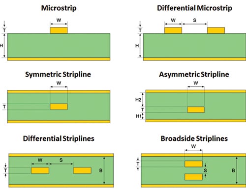
There are a number of variations of those two forms of waveguides out there, as proven in Fig. 2. As a result of complexity of the fabrication of PCBs, broadside and uneven strip traces are seldom used.
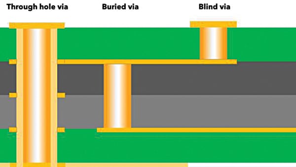
Vias
By way of is vertical interconnect entry. When a sign travels from one layer to a different layer through is used. There are three forms of vias in PCBs.
By-hole vias are those who journey from the highest layer to the underside layer of the PCB. Blind vias are from both the highest or backside layer to an interior layer of the PCB. Buried vias are between two interior layers of the PCB with no entry to them after the PCB manufacturing.
By-hole vias are the commonest. Buried and blind vias are costlier to fabricate. Fig. 3 exhibits various kinds of vias in a vertical cross-section of a PCB.
Selecting PCB Supplies
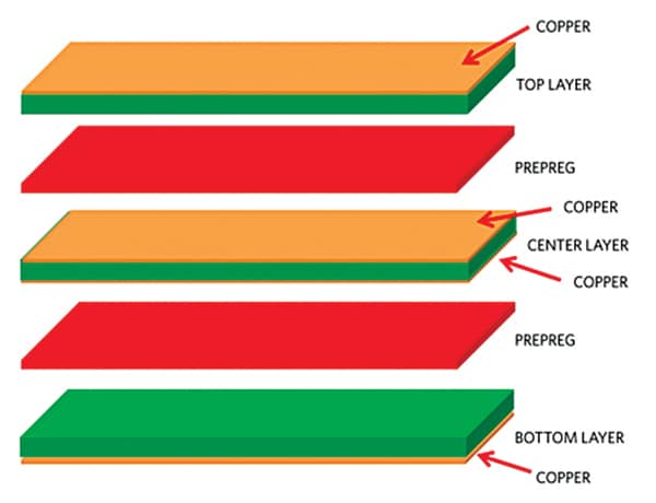
Resulting from manufacturability, high-speed PCB layer depend is mostly a good quantity. The essential elements of PCB manufacturing are core and prepreg.
The core is a layer of dielectric with copper on both facet. The layer of dielectric is fashioned between two clean foils of copper, to a specified thickness. Prepreg, which is an abbreviation for pre-impregnated, is utilized by PCB producers to attach collectively etched cores, or a copper foil to an etched core. Fig. 4 exhibits the development particulars of a 4-layer PCB for example.
The selection of PCB materials is determined by the applying. FR4 (FR stands for Flame Retardant) materials is essentially the most used these days. Nonetheless, very high-speed designs require different supplies like Megtron6.
A couple of parameters that must be saved in thoughts whereas checking varied PCB supplies to be used are:
Dielectric fixed (Dk): The dielectric fixed (Dk) of a PCB materials is mostly between 3.5 and 5.5. A cloth’s Dk stage will often drop because the frequency rises. For a cloth to be secure for high-frequency functions, it should keep a secure dielectric fixed over your complete vary of frequencies of operations.
The upper the relative dielectric fixed, the slower a sign travels on a wire, the decrease the impedance of a given hint geometry, and the bigger the stray capacitance alongside a transmission line. Given a selection, the decrease dielectric fixed is preferable.
Loss tangent: A cloth’s loss tangent provides a measure of the ability misplaced as a result of materials. The decrease a cloth’s loss tangent, the higher is the fabric.
The Tan δ of most PCB supplies ranges from 0.02 for essentially the most used supplies to 0.001 for very-low-loss, high-end supplies. It additionally varies with frequency, growing as frequency will increase. Loss tangent is often a vital consideration at frequencies larger than 1GHz.
Glass transition temperature: Glass transition temperature (Tg) is the temperature vary by which a PCB substrate transitions from a glassy, inflexible state to a softened, deformable state as polymer chains turn into extra cell. When the fabric cools again down, its properties return to their authentic states.
Decomposition temperature: Decomposition temperature (Td) is the temperature at which a PCB materials chemically decomposes (the fabric loses not less than 5% of its mass). A cloth’s Td is a vital ceiling when assembling PCBs, as a result of when a cloth reaches or surpasses its Td, modifications to its properties usually are not reversible.
Select a cloth the place you’ll be able to work in a temperature vary that’s larger than Tg however effectively under Td. Most solder temperatures throughout PCB meeting are within the 200ºC to 250ºC vary and, fortunately, most supplies have a Td larger than 320ºC.
Coefficient of thermal enlargement: The coefficient of thermal enlargement (CTE) is the speed of enlargement of a PCB materials because it heats up. As a cloth’s temperature rises previous Tg, the CTE will rise quickly.
The CTE of a substrate is often a lot larger than copper, which may trigger interconnection points as a PCB is heated. CTE alongside the X and Y axes are typically low—round 10 to twenty ppm/ºC. The CTE alongside the Z-axis ought to be as little as doable, and this may enhance quickly as a cloth surpasses Tg.
To cut back the upper enlargement above Tg, select a cloth with the next Tg, not less than 170ºC, and a low Z-axis CTE at a temperature larger than Tg.
Some Frequent Errors to Keep away from Throughout Excessive-Velocity PCB Design
- Use correct hint width as calculated from the layer stack-up for the required traits impedance.
- For energy and floor traces and planes, the width have to be adequate to hold the present.
- Place decoupling capacitors close to/under the ability pins.
- Make separate grounds for analog and digital indicators.
- Ensure that the reference aircraft for vital indicators is steady finish to finish.
- Observe any particular format suggestions given by the IC producer.
- By no means route delicate digital indicators over high-voltage energy planes.
- For differential sign size tuning, at all times match the uneven facet.
- For prime-speed indicators, reduce the through stub—the unused through portion. For instance, in a sign touring from layer 1 to layer 18 in a 20-layer PCB, the a part of the through in layers 19 and 20 is the stub. Again drilling could also be carried out to take away the stub. However there’s a value penalty.
- Ensure that energy and floor planes increasing in a number of layers are well-stitched by vias. Additionally, don’t place too many vias in a slender space, which can, in flip, enhance the present density and resistance.
- Hold a watch on the anti-pad. The form of the anti-pad usually impacts high-frequency indicators. SI evaluation can counsel an acceptable anti-pad form for the design into consideration.
- Test no traces or planes are routed within the keep-out areas.
- Ensure that the minimal distances specified throughout format (for instance, the spacing between through to through, through to pad, through to hint, and so on) are manufacturable. Contact your PCB fabricator for his or her functionality and value beforehand.
Joyful designing!
Additionally Learn
The writer Arka Mukherjee is a postgraduate and gold medallist from IIT Delhi. He’s an electronics fanatic with greater than a decade of expertise in embedded techniques design for optical entry networks