| Aug 09, 2023 |
|
(Nanowerk Information) Researchers have developed an easy-to-build, low-cost 3D nanoprinting system that may create arbitrary 3D buildings with extraordinarily superb options. The brand new 3D nanoprinting method is exact sufficient to print metamaterials in addition to quite a lot of optical units and elements corresponding to microlenses, micro-optical units and metamaterials.
|
|
“Our system makes use of a two-step absorption course of to comprehend 3D printing with accuracy reaching the nanometer stage, which is appropriate for industrial manufacturing,” mentioned analysis staff chief Cuifang Kuang from the Zhejiang Lab and Zhejiang College, each in China. “It may be used for quite a lot of functions corresponding to printing micro or nanostructures for finding out organic cells or fabricating the specialised optical waveguides used for digital and augmented actuality units.”
|
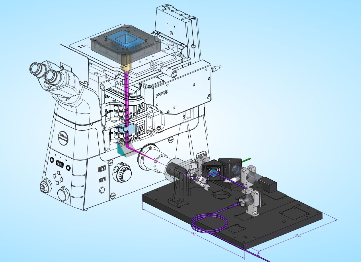 |
| Researchers developed an easy-to-build, low-cost 3D nanoprinting system that may create arbitrary 3D buildings with extraordinarily superb options. It’s appropriate with most industrial microscopes. (Picture: Cuifang Kuang, Zhejiang College)
|
|
Typical high-resolution 3D nanoprinting approaches use pulsed femtosecond lasers that value tens of 1000’s of {dollars}. Within the Optica Publishing Group journal Optics Letters (“Excessive-resolution 3D nanoprinting primarily based on two-step absorption through an built-in fiber-coupled laser diode”), Kuang and colleagues describe their new system primarily based on an built-in fiber-coupled continuous-wave laser diode that’s not solely cheap but additionally simple to function.
|
|
“This new strategy helps make 3D nanoprinting accessible to scientists, even ones who are usually not conversant in the optical techniques usually used for this sort of fabrication,” mentioned Kuang. “It might finally result in low-cost desktop 3D nanoprinting units that would provide precision nanoprinting to anybody.”
|
Making a easy setup
|
|
3D printing objects with a characteristic measurement of roughly 100 nm usually requires a way referred to as two-photon absorption. This entails utilizing costly femtosecond lasers to attain precision 3D photon absorption that solidifies, or polymerizes, a liquid resin that’s delicate to gentle.
|
|
Lately, an strategy referred to as two-step absorption has been developed as an alternative choice to two-photon absorption developed by Vincent Hahn’s analysis staff at Karlsruhe Institute of Know-how. It makes use of a particular photoinitiator referred to as benzil along with a single gentle supply to create polymerization. Within the new work, the researchers developed a simplified and sooner 3D nanoprinting two-step absorption system that makes use of a 405-nm-wavelength built-in fiber-coupled laser.
|
|
For 2D or 3D printing with the brand new system, the laser beam from the single-mode polarization-maintaining fiber is collimated and directed onto galvanometric mirrors. It’s then targeted into the photosensitive materials with a high-numerical aperture microscope goal.
|
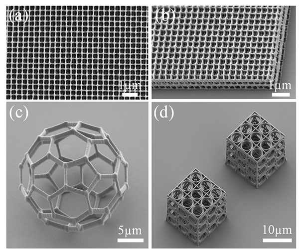 |
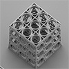
| The researchers used their new system to make quite a lot of detailed 3D buildings, together with a 3D woodpile construction (a & b), a 20-micron-diameter buckyball (c) and two cubical field frames (d). The pictures have been acquired with an electron microscope. (Picture: Cuifang Kuang, Zhejiang College)
|
Printing tiny objects
|
|
“The straightforward system doesn’t want numerous optical elements to modulate the laser beam, which saves cash and produces much less optical aberrations, or errors,” mentioned Kuang. “It is usually extremely steady and appropriate with most industrial microscopes.”
|
|
The researchers display their 3D nanoprinting system by utilizing it at low speeds to print 2D line gratings and 3D woodpile nanostructures with a lateral interval of 350 nm. Utilizing a sooner scan pace of 1000 micron per second, 2D gratings with sub-200-nm decision and sub-50-nm linewidth can nonetheless be fabricated with laser energy lower than 1mW.
|
|
The researchers at the moment are working to enhance the writing pace and high quality of the method whereas sustaining excessive decision. It will make the system sensible to make use of for much more functions.
|
