

Halide perovskites are a household of supplies which have attracted consideration for his or her superior optoelectronic properties and potential functions in units akin to high-performance photo voltaic cells, light-emitting diodes, and lasers.
These supplies have largely been carried out into thin-film or micron-sized machine functions. Exactly integrating these supplies on the nanoscale may open up much more exceptional functions, like on-chip mild sources, photodetectors, and memristors. Nonetheless, reaching this integration has remained difficult as a result of this delicate materials could be broken by typical fabrication and patterning methods.
To beat this hurdle, MIT researchers created a method that enables particular person halide perovskite nanocrystals to be grown on-site the place wanted with exact management over location, to inside lower than 50 nanometers. (A sheet of paper is 100,000 nanometers thick.) The scale of the nanocrystals will also be exactly managed by way of this method, which is essential as a result of dimension impacts their traits. For the reason that materials is grown regionally with the specified options, typical lithographic patterning steps that might introduce harm aren’t wanted.
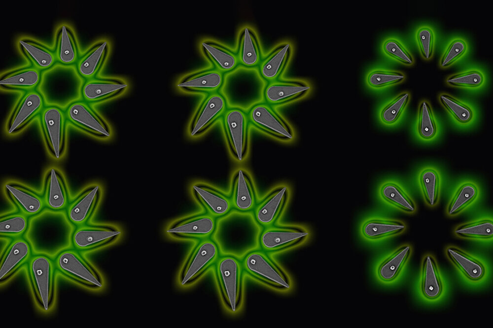
The approach can be scalable, versatile, and suitable with typical fabrication steps, so it could possibly allow the nanocrystals to be built-in into useful nanoscale units. The researchers used this to manufacture arrays of nanoscale light-emitting diodes (nanoLEDs)—tiny crystals that emit mild when electrically activated. Such arrays may have functions in optical communication and computing, lensless microscopes, new varieties of quantum mild sources, and high-density, high-resolution shows for augmented and digital actuality.
“As our work exhibits, it’s important to develop new engineering frameworks for integration of nanomaterials into useful nanodevices. By transferring previous the standard boundaries of nanofabrication, supplies engineering, and machine design, these methods can permit us to govern matter on the excessive nanoscale dimensions, serving to us notice unconventional machine platforms essential to addressing rising technological wants,” says Farnaz Niroui, the EE Landsman Profession Growth Assistant Professor of Electrical Engineering and Laptop Science (EECS), a member of the Analysis Laboratory of Electronics (RLE), and senior creator of a brand new paper describing the work.
Niroui’s co-authors embody lead creator Patricia Jastrzebska-Good, an EECS graduate scholar; Weikun “Spencer” Zhu, a graduate scholar within the Division of Chemical Engineering; Mayuran Saravanapavanantham, Sarah Spector, Roberto Brenes, and Peter Satterthwaite, all EECS graduate college students; Zheng Li, an RLE postdoc; and Rajeev Ram, professor {of electrical} engineering. The analysis might be revealed in Nature Communications.
Tiny crystals, large challenges
Integrating halide perovskites into on-chip nanoscale units is extraordinarily troublesome utilizing typical nanoscale fabrication methods. In a single strategy, a skinny movie of fragile perovskites could also be patterned utilizing lithographic processes, which require solvents which will harm the fabric. In one other strategy, smaller crystals are first fashioned in answer after which picked and positioned from answer within the desired sample.
“In each circumstances there’s a lack of management, decision, and integration functionality, which limits how the fabric could be prolonged to nanodevices,” Niroui says.
As an alternative, she and her group developed an strategy to “develop” halide perovskite crystals in exact places immediately onto the specified floor the place the nanodevice will then be fabricated.
Core to their course of is to localize the answer that’s used within the nanocrystal progress. To take action, they create a nanoscale template with small wells that include the chemical course of by way of which crystals develop. They modify the floor of the template and the within of the wells, controlling a property often called “wettability” so an answer containing perovskite materials will not pool on the template floor and might be confined contained in the wells.
“Now, you’ve got these very small and deterministic reactors inside which the fabric can develop,” she says.
And that’s precisely what occurs. They apply an answer containing halide perovskite progress materials to the template and, because the solvent evaporates, the fabric grows and varieties a tiny crystal in every effectively.
A flexible and tunable approach
The researchers discovered that the form of the wells performs a important function in controlling the nanocrystal positioning. If sq. wells are used, as a result of affect of nanoscale forces, the crystals have an equal probability of being positioned in every of the effectively’s 4 corners. For some functions, that may be adequate, however for others, it’s essential to have a better precision within the nanocrystal placement.
By altering the form of the effectively, the researchers had been capable of engineer these nanoscale forces in such a approach {that a} crystal is preferentially positioned within the desired location.
Because the solvent evaporates contained in the effectively, the nanocrystal experiences a stress gradient that creates a directional power, with the precise path being decided utilizing the effectively’s uneven form.
“This enables us to have very excessive precision, not solely in progress, but in addition within the placement of those nanocrystals,” Niroui says.
Additionally they discovered they may management the dimensions of the crystal that varieties inside a effectively. Altering the dimensions of the wells to permit kind of progress answer inside generates bigger or smaller crystals.
They demonstrated the effectiveness of their approach by fabricating exact arrays of nanoLEDs. On this strategy, every nanocrystal is made right into a nanopixel which emits mild. These high-density nanoLED arrays may very well be used for on-chip optical communication and computing, quantum mild sources, microscopy, and high-resolution shows for augmented and digital actuality functions.
Sooner or later, the researchers need to discover extra potential functions for these tiny mild sources. Additionally they need to check the bounds of how small these units could be, and work to successfully incorporate them into quantum techniques. Past nanoscale mild sources, the method additionally opens up different alternatives for growing halide perovskite-based on-chip nanodevices.
Their approach additionally supplies a neater approach for researchers to check supplies on the particular person nanocrystal stage, which they hope will encourage others to conduct further research on these and different distinctive supplies.
“Learning nanoscale supplies by way of high-throughput strategies typically requires that the supplies are exactly localized and engineered at that scale,” Jastrzebska-Good provides. “By offering that localized management, our approach can enhance how researchers examine and tune the properties of supplies for numerous functions.”
Extra data:
On-site progress of perovskite nanocrystal arrays for built-in nanodevices, Nature Communications (2023).
Offered by
Massachusetts Institute of Know-how
Quotation:
Researchers develop exact arrays of nanoscale LEDs (2023, July 6)
retrieved 6 July 2023
from https://phys.org/information/2023-07-precise-arrays-nanoscale.html
This doc is topic to copyright. Other than any truthful dealing for the aim of personal research or analysis, no
half could also be reproduced with out the written permission. The content material is offered for data functions solely.