
Over the past half-century, we’ve come to think about Moore’s Regulation—the roughly biennial doubling of the variety of transistors in a given space of silicon, the beneficial properties that drive computing ahead—as one thing that simply occurs, as if it had been a pure, inevitable course of, akin to evolution or growing old. The truth, after all, is way completely different. Holding tempo with Moore’s Regulation requires nearly unimaginable expenditures of time, power, and human ingenuity—hundreds of individuals on a number of continents and limitless acres of a few of the most advanced equipment on the planet.
Maybe probably the most important of those machines performs
extreme-ultraviolet (EUV) photolithography. EUV lithography, the product of a long time of R&D, is now the driving expertise behind the previous two generations of cutting-edge chips, utilized in each top-end smartphone, pill, laptop computer, and server within the final three years. But Moore’s Regulation should march on, and chipmakers proceed to advance their street maps, that means they’ll must shrink gadget geometries even additional.
So at
ASML, my colleagues and I are growing the subsequent technology of lithography. Referred to as high-numerical-aperture EUV lithography, it entails a serious overhaul of the system’s inner optics. Excessive-NA EUV ought to be prepared for industrial use in 2025, and chipmakers are relying on its capabilities to maintain their promised advances by the tip of this decade
The three components of photolithography
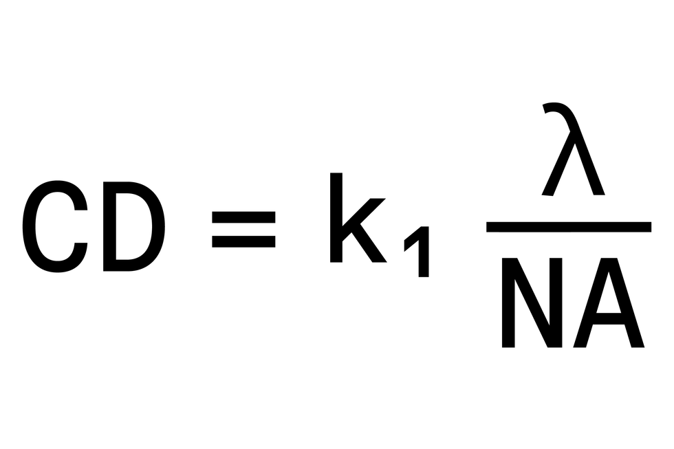
Moore’s Regulation depends on bettering the decision of photolithography so chipmakers can lay down finer and finer circuits. Over the past 35 years, engineers have achieved a decision discount of two orders of magnitude by engaged on a mixture of three components: the wavelength of the sunshine; ok
1, a coefficient that encapsulates process-related components; and numerical aperture (NA), a measure of the vary of angles over which the system can emit gentle.
 Supply: IEEE Spectrum
The essential dimension—that’s, the smallest potential characteristic measurement you’ll be able to print with a sure photolithography-exposure instrument—is proportional to the wavelength of sunshine divided by the numerical aperture of the optics. So you’ll be able to obtain smaller essential dimensions by utilizing both shorter gentle wavelengths or bigger numerical apertures or a mixture of the 2. The ok
1 worth may be pushed as shut as potential to its bodily decrease restrict of 0.25 by bettering manufacturing-process management, for instance.
Usually, probably the most economical methods to spice up decision are by growing the numerical aperture and by bettering instrument and course of management to permit for a smaller ok
1. Solely after chipmakers run out of choices to additional enhance NA and ok1 do they resort to lowering the wavelength of the sunshine supply.
However, the trade has needed to make that wavelength change quite a lot of instances. The historic development of wavelengths went from 365 nanometers, generated utilizing a mercury lamp, to 248 nm, through a krypton-fluoride laser, within the late Nineteen Nineties, after which to 193 nm, from an argon-fluoride laser, at first of this century. For every technology of wavelength, the numerical aperture of lithography techniques was progressively elevated earlier than trade jumped to a shorter wavelength.
For instance, as using 193 nm was coming to an finish, a novel method to growing NA was launched:
immersion lithography. By inserting water between the underside of the lens and the wafer, the NA might be considerably enlarged from 0.93 to 1.35. From its introduction round 2006, 193-nm immersion lithography was the trade workhorse for modern lithography
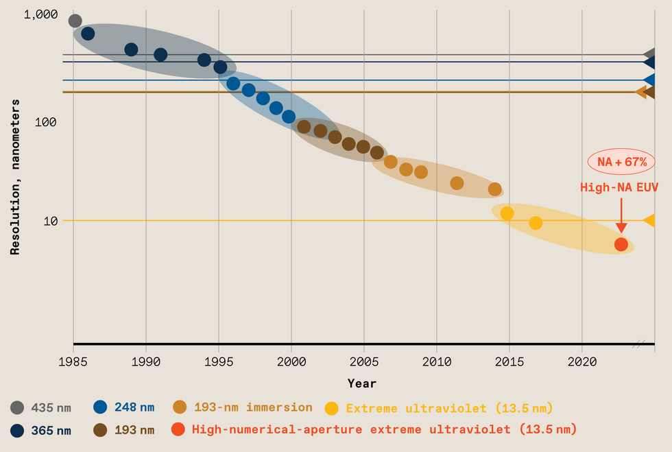 The decision of photolithography has improved about 10,000-fold during the last 4 a long time. That’s due partly to utilizing smaller and smaller wavelengths of sunshine, however it has additionally required higher numerical aperture and improved processing strategies.Supply: ASML
The daybreak of EUV
However as the necessity to print options smaller than 30 nm elevated, and since the NA of 193-nm lithography had been maxed out, maintaining with Moore’s Regulation grew an increasing number of advanced. To create options smaller than 30 nm requires both utilizing a number of patterns to supply a single layer of chip options—a technologically and economically burdensome approach—or one other change of wavelength. It took greater than 20 years and an
unparalleled improvement effort to deliver the subsequent new wavelength on-line: 13.5-nm EUV.
EUV necessitates a wholly new strategy to generate gentle. It’s a remarkably advanced course of that entails hitting molten tin droplets in midflight with a strong CO2 laser. The laser vaporizes the tin right into a plasma, emitting a spectrum of photonic power. From this spectrum, the EUV optics harvest the required 13.5-nm wavelength and direct it by a collection of mirrors earlier than it’s mirrored off a patterned masks to venture that sample onto the wafer. And all of this have to be accomplished in an ultraclean vacuum, as a result of the 13.5-nm wavelength is absorbed by air. (In earlier generations of photolithography, gentle was directed by the masks to venture a sample onto the wafer. However EUV is so readily absorbed that the masks and different optics have to be reflective as a substitute.)
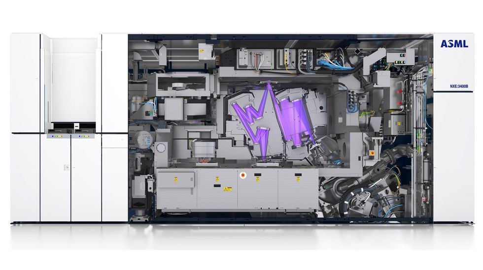 In a vacuum chamber, EUV gentle [purple] displays off a number of mirrors earlier than bouncing off the photomask [top center]. From there the sunshine continues its journey till it’s projected onto the wafer [bottom center], carrying the photomask’s sample. The illustration reveals at present’s industrial system with a 0.33 numerical aperture. The optics in future techniques, with an NA of 0.55, will probably be completely different.Supply: ASML
The swap to EUV from 193-nanometer gentle did a part of the job of lowering the essential dimension. A course of known as “design for manufacturing,” which entails setting the design guidelines of circuit blocks to make the most of photolithography’s limits, has accomplished loads to scale back ok
1. Now it’s time to spice up numerical aperture once more, from at present’s 0.33 to 0.55.
Making high-NA EUV work
Growing the NA from at present’s 0.33 to the goal worth of 0.55 inevitably entails a cascade of different changes. Projection techniques like EUV lithography have an NA on the wafer and in addition on the masks. Once you enhance the NA on the wafer, it additionally will increase the NA on the masks. Consequently, on the masks, the incoming and outgoing cones of sunshine turn out to be bigger and have to be angled away from one another to keep away from overlapping. Overlapping cones of sunshine produce an uneven diffraction sample, leading to disagreeable imaging results.
However there’s a restrict to this angle. As a result of the reflective masks wanted for EUV lithography are literally made from a number of layers of fabric, you’ll be able to’t guarantee getting a correct reflection above a sure reflective angle. EUV masks have a most reflective angle of 11 levels. There are different challenges as effectively, however reflective angle is the largest.
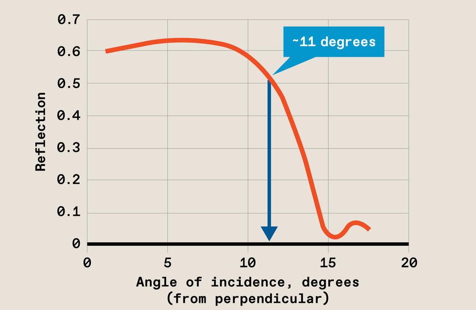 If the EUV gentle strikes the photomask at too steep an angle, it is not going to mirror correctly.Supply: ASML
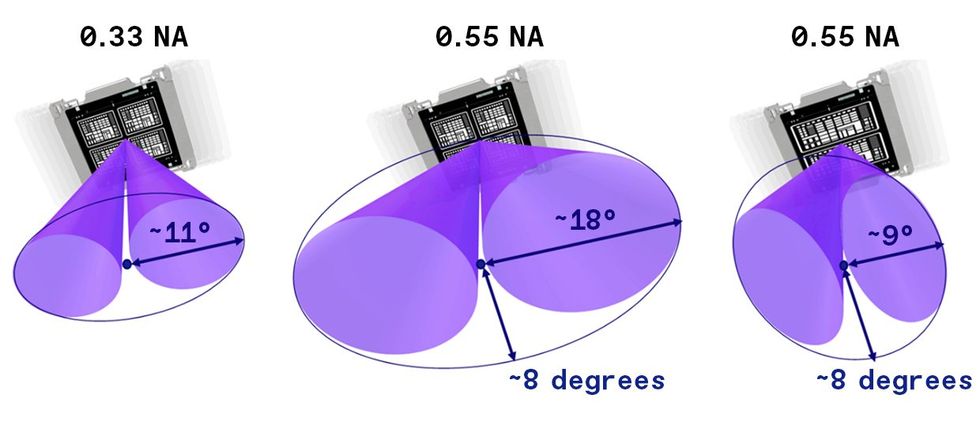 The angle of reflection on the masks in at present’s EUV is at its restrict [left] Growing the numerical aperture of EUV would lead to an angle of reflection that’s too large [center]. So high-NA EUV makes use of anamorphic optics, which permit the angle to extend in just one course [right]. The sector that may be imaged this manner is half the scale, so the sample on the masks have to be distorted in a single course, however that’s ok to take care of throughput by the machine.Supply: ASML
The one strategy to overcome this problem is to extend a top quality known as demagnification. Demagnification is strictly what it appears like—taking the mirrored sample from the masks and shrinking it. To compensate for the reflective-angle drawback, my colleagues and I needed to double the demagnification to 8x. As a consequence, the a part of the masks imaged will probably be a lot smaller on the wafer. This smaller picture area means it should take longer to supply the whole chip sample. Certainly, this requirement would scale back the throughput of our high-NA scanner to beneath 100 wafers per hour—a productiveness degree that may make chip manufacturing uneconomical.
Fortunately, we discovered that it’s mandatory to extend the demagnification in just one course—the one through which the most important reflective angles happen. The demagnification within the different course can stay unchanged. This leads to a suitable area measurement on the wafer—about half the scale utilized in at present’s EUV techniques, or 26 by 16.5 millimeters as a substitute of 26 by 33 mm. This type of direction-dependent, or anamorphic, demagnification kinds the premise of our high-NA system. The optics producer Carl Zeiss has made a herculean effort to design and manufacture an anamorphic lens with the specs required for our new machine.
To make sure the identical productiveness ranges with the half-size area, we needed to redevelop the system’s reticle and wafer levels—the platforms that maintain the masks and wafer, respectively—and transfer them in sync with one another because the scanning course of takes place. The redesign resulted in nanometer-precision levels with acceleration improved by an element of 4.
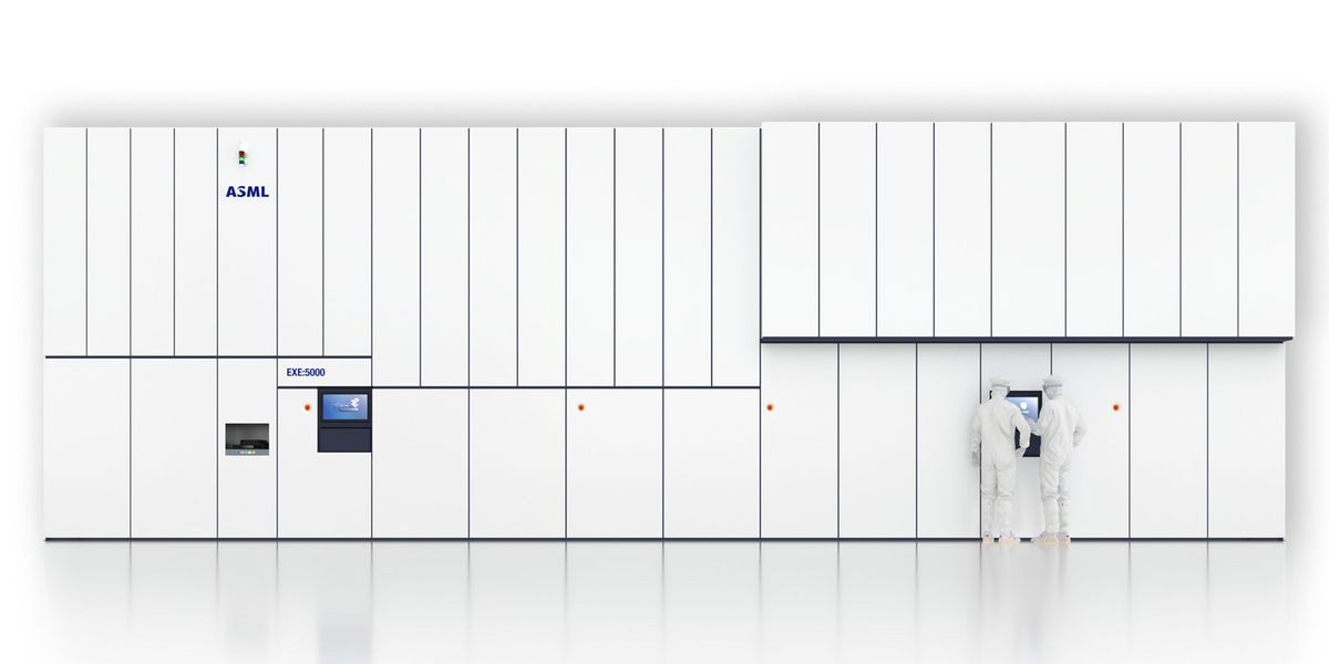
Excessive-NA EUV in manufacturing in 2025
The primary high-NA EUV system, the ASML EXE:5000, will probably be put in in a brand new lab that we’re opening collectively with the Belgium-based nanoelectronics analysis facility Imec, in early 2024. This lab will enable clients, masks makers, photoresist suppliers, and others to develop the infrastructure wanted to make high-NA EUV a actuality.
And it’s important that we do make it a actuality, as a result of high-NA EUV is a essential part in holding Moore’s Regulation alive. Attending to 0.55 NA received’t be the ultimate step, although. From there, ASML, Zeiss, and your entire semiconductor ecosystem will probably be stretching even additional towards applied sciences which can be higher, sooner, and modern in methods we will hardly think about but.
From Your Website Articles
Associated Articles Across the Net