| Jun 29, 2023 |
|
(Nanowerk Information) The info facilities and high-performance computer systems that run synthetic intelligence packages, resembling giant language fashions, aren’t restricted by the sheer computational energy of their particular person nodes. It’s one other drawback — the quantity of knowledge they’ll switch among the many nodes — that underlies the “bandwidth bottleneck” that at the moment limits the efficiency and scaling of those methods.
|
|
The nodes in these methods may be separated by a couple of kilometer. Since metallic wires dissipate electrical indicators as warmth when transferring knowledge at excessive speeds, these methods switch knowledge by way of fiber-optic cables. Sadly, a number of vitality is wasted within the means of changing electrical knowledge into optical knowledge (and again once more) as indicators are despatched from one node to a different.
|
|
In a examine revealed in Nature Photonics (“Massively scalable Kerr comb-driven silicon photonic hyperlink”), researchers at Columbia Engineering exhibit an energy-efficient methodology for transferring bigger portions of knowledge over the fiber-optic cables that join the nodes. This new know-how improves on earlier makes an attempt to transmit a number of indicators concurrently over the identical fiber-optic cables. As an alternative of utilizing a unique laser to generate every wavelength of sunshine, the brand new chips require solely a single laser to generate tons of of distinct wavelengths of sunshine that may concurrently switch unbiased streams of knowledge.
|
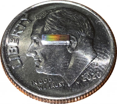 |
| Photonic built-in chip on a dime. (Picture: Lightwave Analysis Laboratory, Columbia Engineering)
|
A less complicated, extra energy-efficient methodology for knowledge switch
|
|
The millimeter-scale system employs a way known as wavelength-division multiplexing (WDM) and gadgets known as Kerr frequency combs that take a single colour of sunshine on the enter and create many new colours of sunshine on the output. The vital Kerr frequency combs developed by Michal Lipson, Higgins Professor of Electrical Engineering and Professor of Utilized Physics, and Alexander Gaeta, David M. Rickey Professor of Utilized Physics and Supplies Science and Professor of Electrical Engineering, allowed the researchers to ship clear indicators via separate and exact wavelengths of sunshine, with area in between them.
|
|
“We acknowledged that these gadgets make supreme sources for optical communications, the place one can encode unbiased data channels on every colour of sunshine and propagate them over a single optical fiber,” says senior writer Keren Bergman, Charles Batchelor Professor of Electrical Engineering at Columbia Engineering, the place she additionally serves as the school director of the Columbia Nano Initiative. This breakthrough might permit methods to switch exponentially extra knowledge with out utilizing proportionately extra vitality.
|
|
The crew miniaturized the entire optical parts onto chips roughly a number of millimeters on every edge for producing gentle, encoded them with electrical knowledge, after which transformed the optical knowledge again into {an electrical} sign on the goal node. They devised a novel photonic circuit structure that permits every channel to be individually encoded with knowledge whereas having minimal interference with neighboring channels. Meaning the indicators despatched in every colour of sunshine don’t turn into muddled and troublesome for the receiver to interpret and convert again into digital knowledge.
|
|
“On this means, our method is rather more compact and energy-efficient than comparable approaches,” says the examine’s lead writer Anthony Rizzo, who performed this work whereas a PhD scholar within the Bergman lab and is now a analysis scientist on the U.S. Air Power Analysis Laboratory Info Directorate. “It’s also cheaper and simpler to scale because the silicon nitride comb era chips may be fabricated in commonplace CMOS foundries used to manufacture microelectronics chips moderately than in costly devoted III-V foundries.”
|
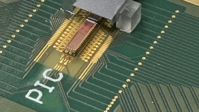 |
| Photonic transmitter chip mounted on a printed circuit board with electrical and fiber optic connections. (Picture: Lightwave Analysis Laboratory, Columbia Engineering)
|
|
The compact nature of those chips allows them to instantly interface with laptop electronics chips, enormously decreasing the entire vitality consumption because the electrical knowledge indicators solely should propagate over millimeters of distance moderately than tens of centimeters.
|
|
Bergman famous, “What this work reveals is a viable path in direction of each dramatically decreasing the system vitality consumption whereas concurrently rising the computing energy by orders of magnitude, permitting synthetic intelligence purposes to proceed to develop at an exponential price with minimal environmental influence.”
|
Thrilling outcomes pave the way in which to real-world deployment
|
|
In experiments, the researchers managed to transmit 16 gigabits per second per wavelength for 32 distinct wavelengths of sunshine for a complete single-fiber bandwidth of 512 Gb/s with lower than one bit in error out of 1 trillion transmitted bits of knowledge. These are extremely excessive ranges of pace and effectivity. The silicon chip transmitting the info measured simply 4 mm x 1 mm, whereas the chip that acquired the optical sign and transformed it into {an electrical} sign measured simply 3 mm x 1 mm—each smaller than a human fingernail.
|
|
“Whereas we used 32 wavelength channels within the proof-of-principle demonstration, our structure may be scaled to accommodate over 100 channels, which is effectively throughout the attain of ordinary Kerr comb designs,” Rizzo provides.
|
|
These chips may be fabricated utilizing the identical amenities used to make the microelectronics chips present in a regular shopper laptop computer or cellphone, offering a simple path to quantity scaling and real-world deployment.
|
|
The subsequent step on this analysis is to combine the photonics with chip-scale driving and management electronics to additional miniaturize the system.
|
