
Hey guys! Right this moment I get to share some superior information with y’all on this first portion of a PCB design mini-series we now have lined up! To begin off, we’re going to take a look at what it takes to create a easy circuit on EasyEDA; let’s dive in!

What good is PCB design?
Nice query! Having the ability to create your individual PCBs on your initiatives is a brilliant helpful ability; it could actually lower the quantity of wire administration wanted, present safe and/or everlasting connections, and will be personalized in many various methods, from enjoyable kind components to shapes that match and even mount to present enclosures. All in all, it’s an superior technique to carry your initiatives to the following degree!
So, what’s EasyEDA?
EasyEDA is the best! It’s a free-to-use, on-line PCB design software program that works in tandem with LCSC for part footprints and provide, in addition to with JLCPCB for manufacturing your designs. These are two superior firms that we work with right here at SparkFun as effectively to carry our new merchandise to you! What’s extra is as a result of these three all work collectively, you may order components from LCSC similtaneously your boards from JLCPCB, and so they even supply an choice to obtain your boards totally assembled, with your whole parts hooked up and applications uploaded (which is particularly helpful when designing surface-mount boards, however we’ll get to that within the subsequent portion of this mini-series).
That’s so cool! Inform me all of the issues!
Woohoo! Okay, let’s get began! First issues first, you’re going to wish to create an account with EasyEDA. When you confirm your e-mail handle, go forward and open up a brand new tab, navigate to EasyEDA, and login from there. The timeout to login web page that comes after verifying your e-mail will be finicky so it’s finest to only login from the EasyEDA homepage. While you’re logged in, navigate to the ‘EasyEDA Designer’ and choose ‘Customary Version’ when prompted. This could open up a brand new tab and also you’ll be capable of create a brand new challenge inside the designer; with all that accomplished, you must see a display screen like this:

That is your schematic web page! Right here is the place we are going to design the circuit and let this system understand how we wish issues related. A number of fast navigation suggestions for working on this house: the scroll wheel will help you zoom in to the canvas, and proper clicking and dragging will help you transfer it round.
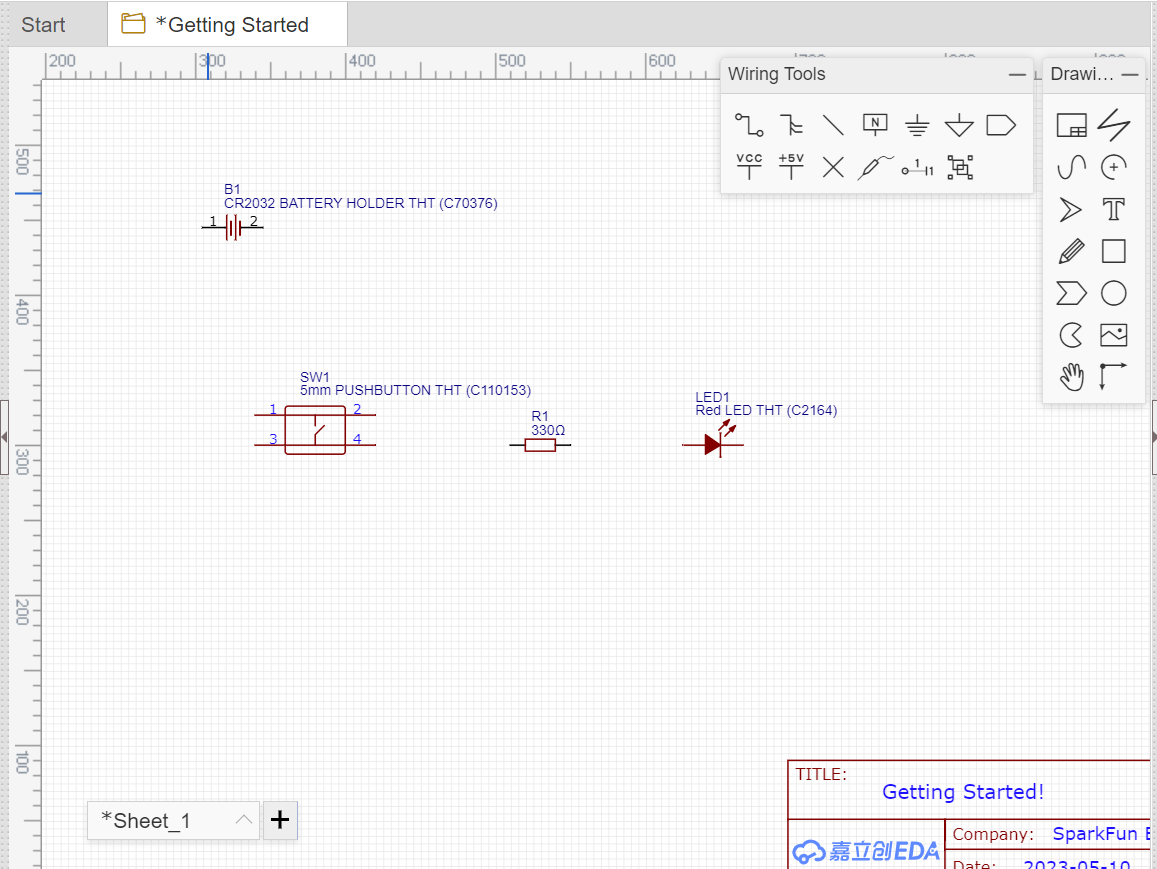
Now let’s get some parts in right here! We’re simply going to do a extremely easy circuit to get accustomed to how this works, so we’ll want a battery, a button, a resistor, and an LED. Hit “Shift + F” to open up the library search web page. There’s a pair other ways to do that: we will search utilizing key phrases inside the EasyEDA engine, or, and that is the best way I want to do it, we will search utilizing product codes from LCSC.
That is now built-in to the EasyEDA library search web page and will be accessed by deciding on the LCSC Electronics possibility on the prime left of the window. Since we’re simply beginning out, I’d suggest simply going to LCSC and looking out from their web site, because it’s just a little cramped to take action inside the designer. Take a while to test all of that out and get accustomed to discover what you want!
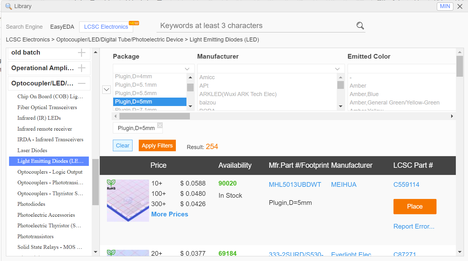
For in the present day, I’ll present the product codes I used beneath:
- Battery Holder: C70376
- Button: C110153
- Resistor: C58608
- LED: C2164
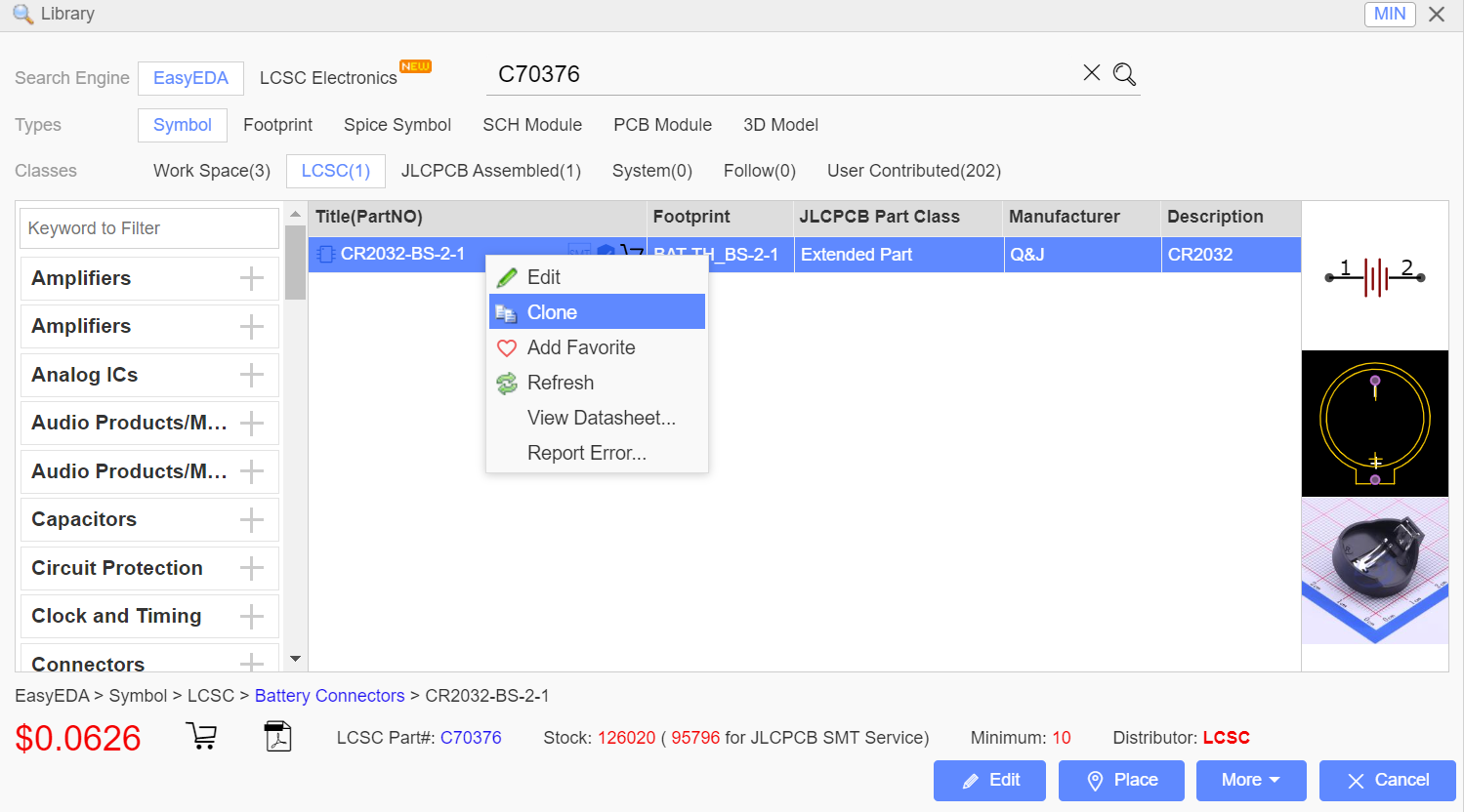
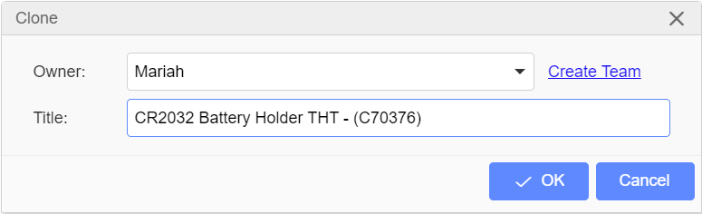
What’s tremendous helpful is that you’ll be able to ‘Clone’, rename, and save parts to your individual private library to have available the following time you want them! I have a tendency to offer it a typical identify that I exploit for the half, whether or not or not it’s THT or SMT (through-hole know-how, which pokes by way of the board and is soldered on the bottom, or surface-mount know-how, which rests on the face of the board and is soldered to pads on that aspect), and the LCSC product code. That’s simply what I do, however you’re welcome to do what works finest for you!
Go forward and place every of the components we’re working with into your schematic!
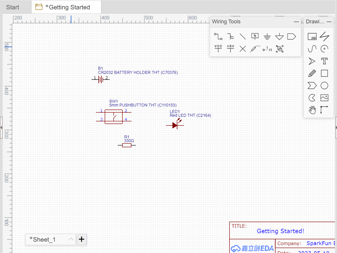
Yay! We’ve all our little buddies, able to go! Let’s rearrange them a bit to make our connections just a little simpler (consider this as your “breadboarding stage”, it’s a really related course of):
Chances are you’ll be questioning, “Mariah, why the heck is the battery so distant from every little thing else? Don’t we want it to energy this entire factor?” Sure, we do! So, let’s speak about that: we might run all of our connections to the battery as we might on a breadboard, however in a extra difficult circuit that may develop into quite a lot of issues needing to hook up with energy and actually bundle up our schematic.
So, what will we do? Nicely, much like utilizing energy and floor rails on a breadboard for issues to attach again to, we now have VCC and GND flags for our schematic. Flags are a helpful instrument that permit us to make connections on a schematic with out having to attract all of it the best way out; so so long as our battery is related to VCC and GND, every little thing else that’s related to a kind of flags can be related to our battery!
Go forward and seize, first, the VCC flag from the ‘Wiring Instruments’ bar; we’ll place one by our battery, and one by our button (this can permit us to regulate when energy goes from the battery to the LED with the button). Subsequent, we’ll seize the GND flag and place one on the opposite aspect of the battery, and one on the far aspect of the LED, like so:
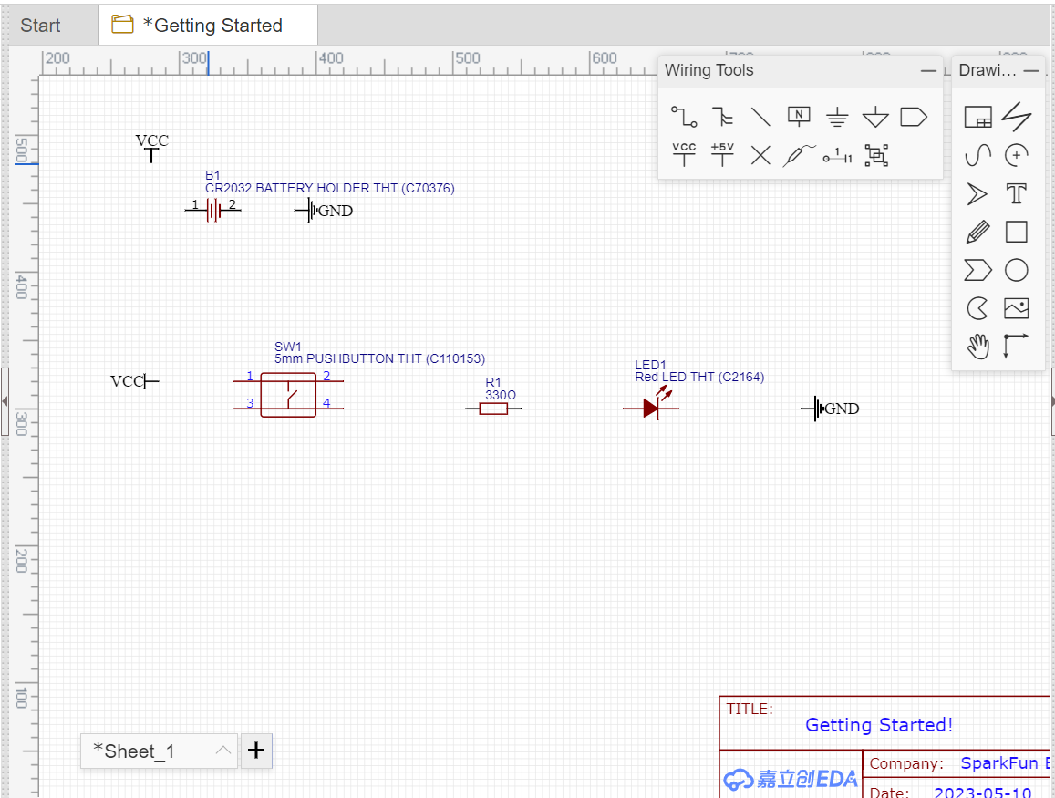
Now all that’s left is to make our connections! The ‘Z’ wanting form with a circle on every finish is our wire instrument, which it’s also possible to entry by urgent ‘W’ (use the ESC key to exit the instrument). To be sure to’re connecting issues, hover over the half till you see just a little circle pop up; that is to point that the wire you’re drawing is to be hooked up to that half.

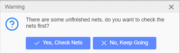
And with that, we’ve accomplished our first schematic diagram! Right here comes the tremendous enjoyable half: on the prime of your display screen, hover over the ‘Design’ possibility and choose ‘Convert Schematic to PCB’. This may set off a popup that asks if you wish to ‘Test Nets’; primarily what that does is say, “Hey! You might have some unused connections in your diagram!” However we don’t wish to use each doable connection obtainable on our parts, though it might be good to double test that we did certainly make those we meant to. Should you’d prefer to see that course of, go forward and permit it to run, in any other case we’ll say, “No, thanks!” and transfer on. One other window will popup and ask plenty of questions that we don’t want to fret about for our functions in the present day, so simply exit out of that.
That is the PCB design house! The pink rectangle you see is our board define and would be the dimension and form of our completed board; that is auto-generated based mostly on the scale and variety of parts we now have, and will be personalized! However we’ll keep on with this for now. You might also discover the blue traces criss-crossing over our components; these are known as “Rat’s Nest Traces” and present us how we wished issues related based mostly on our schematic diagram.
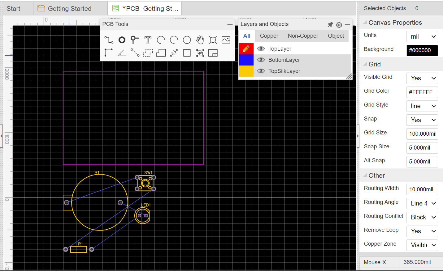
Nevertheless, earlier than we will begin doing that, we have to lay out our parts how we wish them on our board. I favored this setup with the battery on the left and our button and lightweight on the precise, however you are able to do no matter you want (use ‘R’ to rotate parts)!
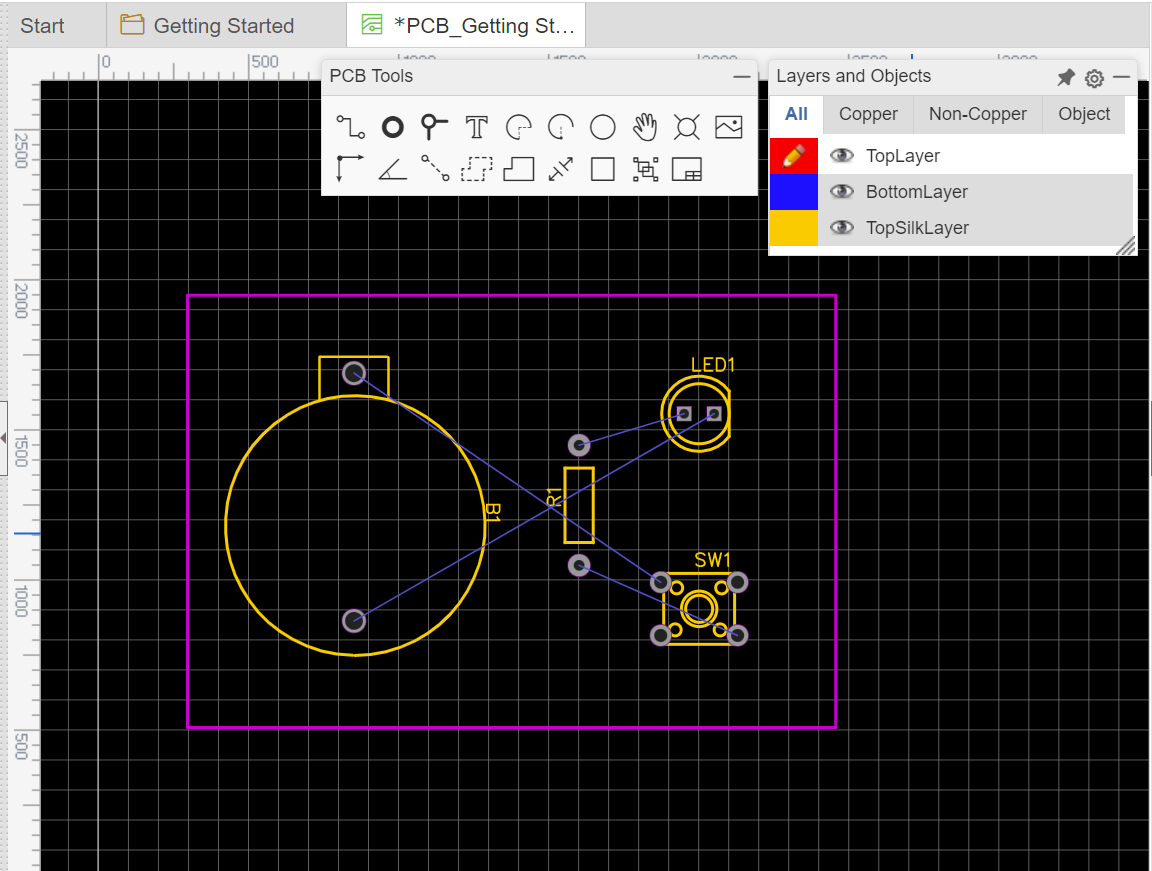
Now that issues are the place we wish them to be, we will begin making our connections! Similar to on the schematic, you may both choose the wire instrument from the toolbar, or press ‘W’ as a shortcut (just be sure you have ‘Prime Layer’ chosen below the ‘Layers and Objects’ menu). Then we simply choose no matter pad we wish to begin with, and that Rat’s Nest Line will spotlight, letting us know the place it wants to attach subsequent! I began by connecting the battery to the button, and the resistor to the LED.
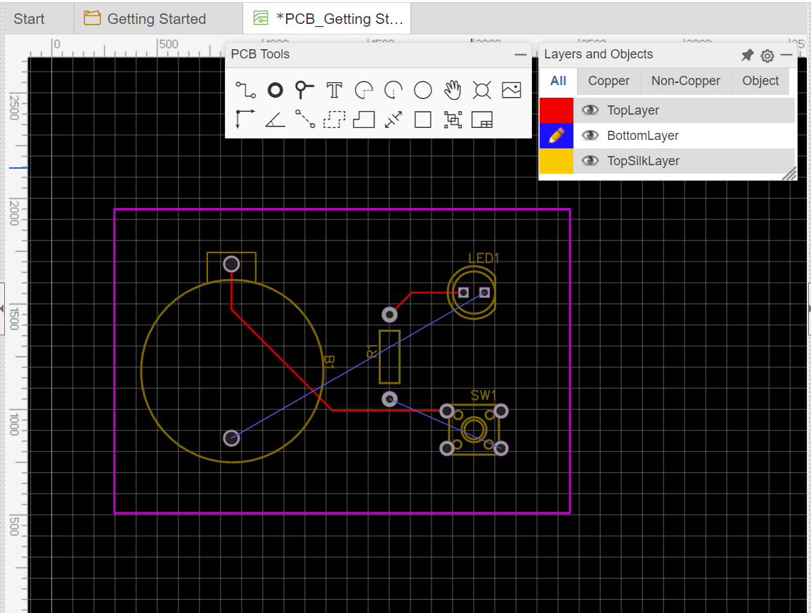
Chances are you’ll discover right here that the final couple connections are intersecting with the traces we’ve simply made; this isn’t nice as a result of crossed traces means crossed connections, and meaning a dud board and even short-circuiting. So, what ought to we do? There’s two choices: we might go alllllll the best way round our present traces to attach the final Rat’s Nest Traces, or we might do one thing fancy.
Below the ‘Layers and Objects’ menu, choose the blue sq. the place it says ‘Backside Layer’; this can permit us to create traces on the opposite aspect of the board, going safely below our present prime layer traces! This can be a profit to designing with THT in that, because the parts undergo the board, they are often accessed by traces from each the highest and backside.
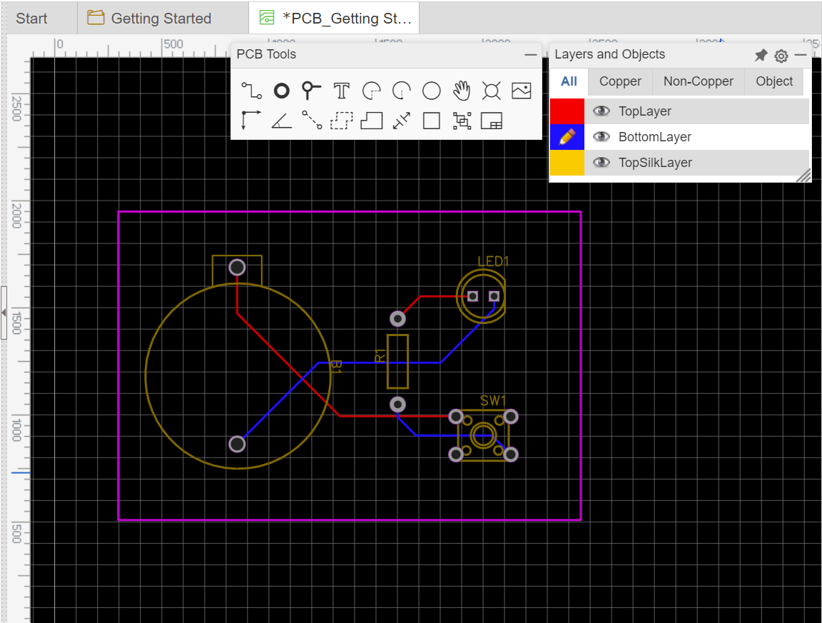
And that’s all of our connections made! You’ve simply designed a totally purposeful PCB for the primary time! Let’s take one final have a look at one thing earlier than we go, and that’s the ‘Prime Silk Layer’, or the yellow possibility on the ‘Layers and Objects’ menu. I wasn’t an enormous fan of the place the part IDs have been positioned on this layer, so I made a decision to vary these up a bit.
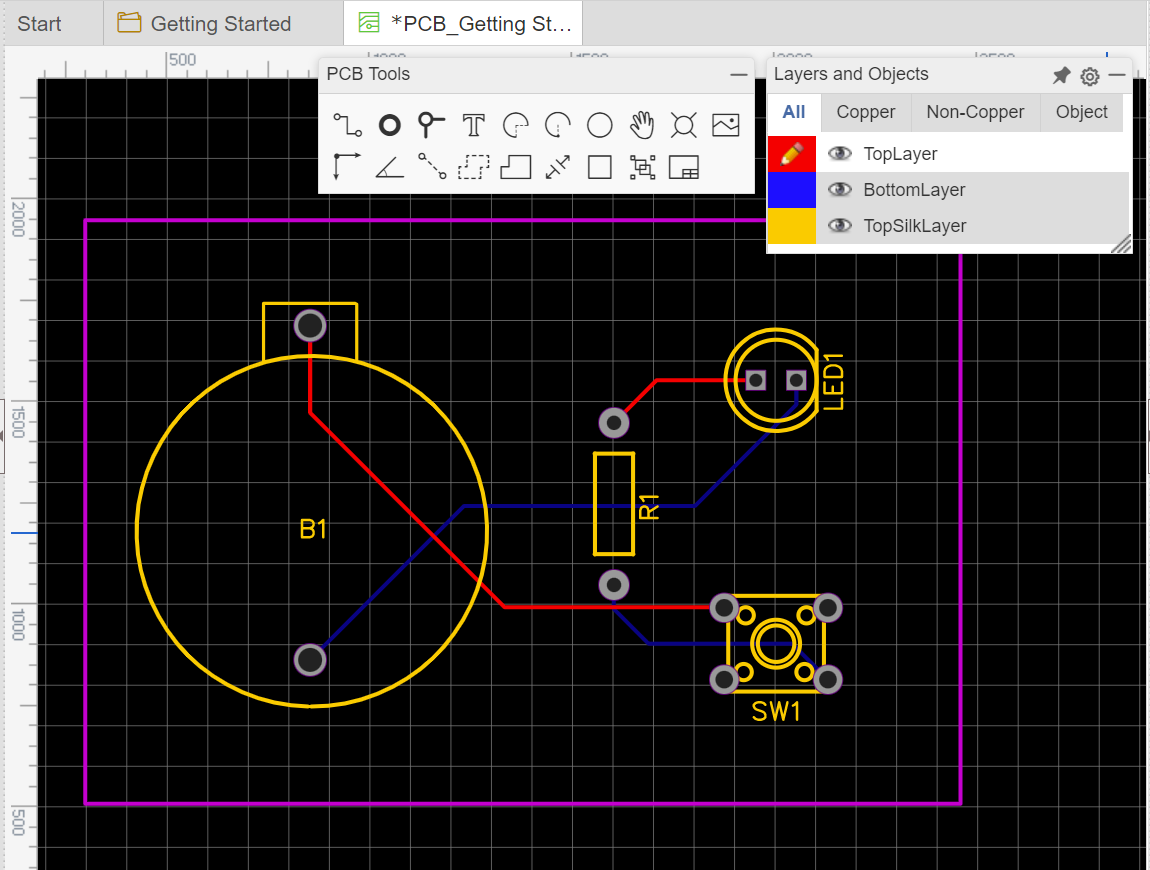
Now, not solely can we manipulate present silk layer textual content, however we will create our personal! With ‘Prime Silk Layer’ energetic, choose the ‘T’ instrument from the ‘PCB Instruments’ menu; this can generate ‘TEXT’ that we will change to say no matter we like.


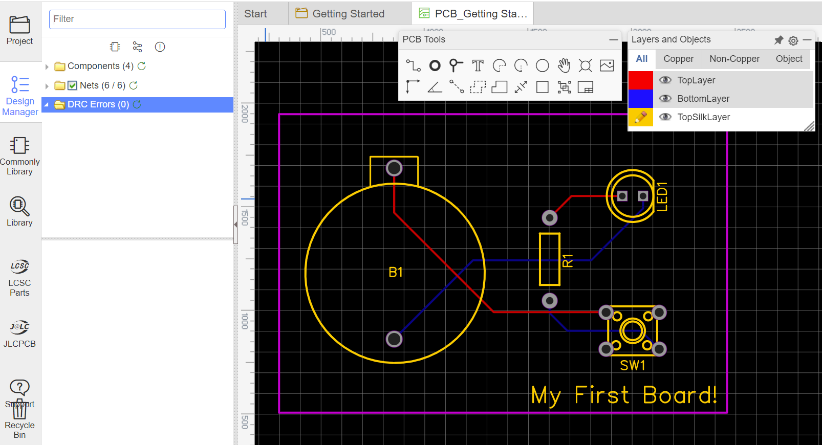
If we had a extra difficult circuit, it might be exhausting to inform if we’ve accomplished all we meant to. One technique to test on that’s to hover over the ‘Design’ tab on the prime, and choose ‘Test DRC’ (DRC stands for ‘Design Guidelines Test’ which seems for issues like crossed traces, missed connections, and so forth).
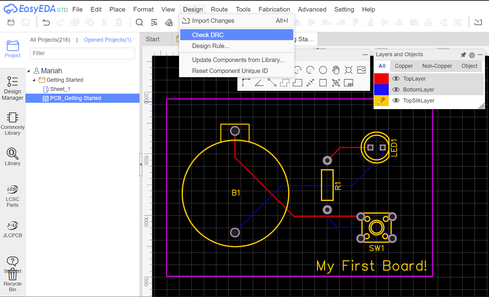
As you may see on the left, we now have no DRC errors, all the parts we wished, and we’ve made each connection that we laid out on our schematic diagram!
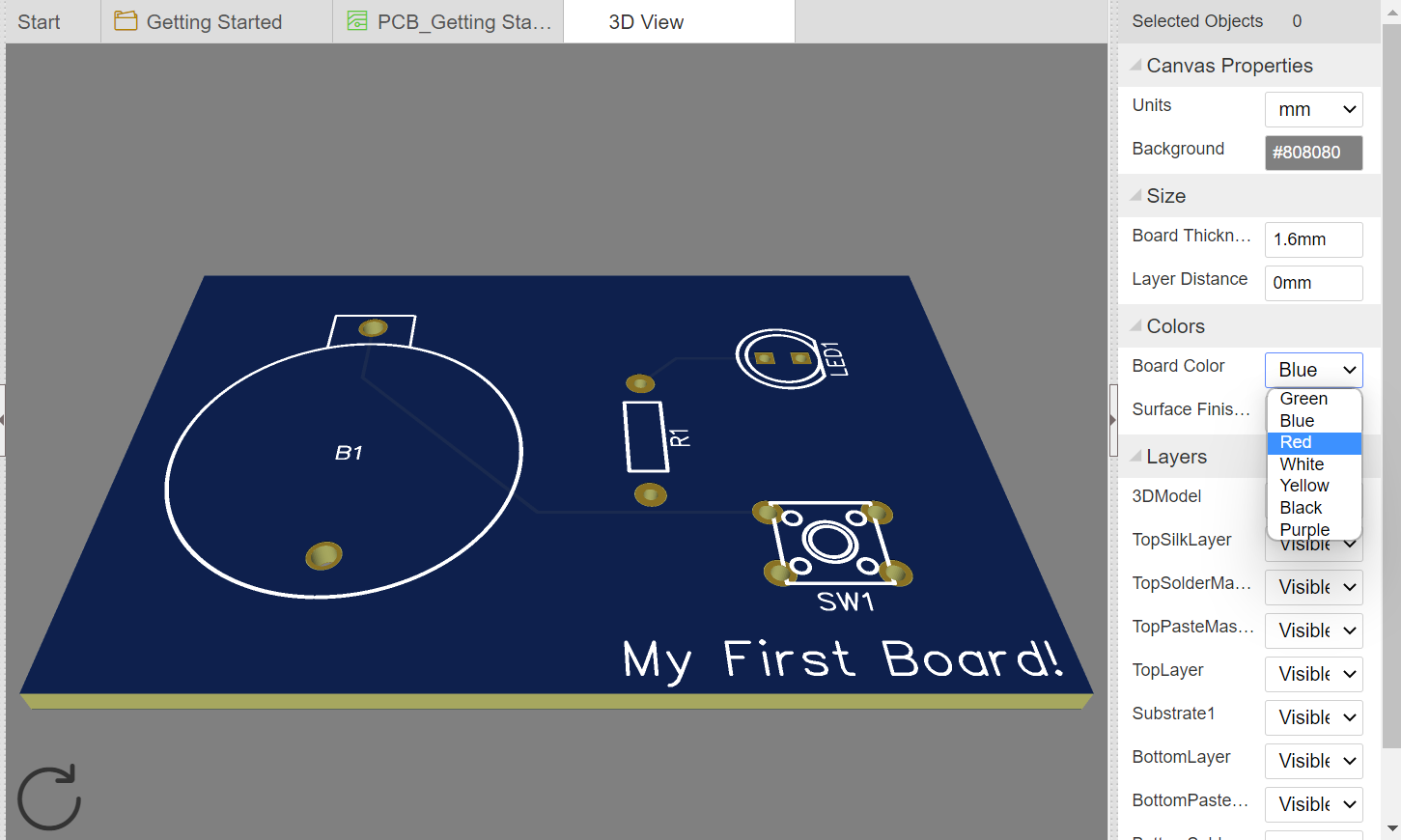
That’s all there may be to it! Your board is able to be manufactured! However what colour ought to it’s? If solely there was a technique to visualize what it’d seem like… Nicely, guess what? There may be!! Hover over the ‘View’ tab on the prime of the display screen, and choose ‘3D View’; this can create a digital PCB based mostly on our design!

From right here we will manipulate the traits of our board, comparable to the colour and pad varieties. It begins out blue, however I actually just like the pink and black one of the best (the black colour possibility is available in a matte slightly than gloss just like the others), so I’m gonna change it to pink; try every of the colour choices and select your favourite!
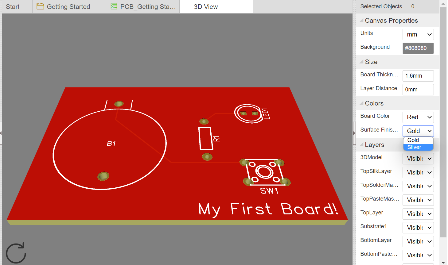
Since it is a 3D view, we will even rotate our board round and take a look at how the again seems; right here we will even see the underside layer traces that we made!

That’s so enjoyable! How can I study extra?
I’m so excited to get to share this course of with y’all; creating PCBs is one in every of my favourite issues to do and I encourage you to mess around with this program. Preserve an eye fixed out for the following installment of this mini-series the place I’ll stroll you thru designing with surface-mount know-how! And please share your PCB initiatives with us, and let me know in case you have any questions or want to see one thing particular transferring ahead, and I’ll do my finest to offer solutions and/or examples; welcome to the vast world of PCB design!
Go away a remark beneath, or discover us on Twitter, Instagram, Fb or LinkedIn.