
And we’re again! At the moment we’re going to wrap up our PCB design sequence with having a look on the extra inventive, customizable features of design. This includes altering up our board form, importing pictures on to the silk display, and studying the best way to add mounting holes for issues like keyrings or stand-offs. That is my favourite kind of board design to do, so let’s get this ball rolling!
In case you missed it: you should definitely take a look at the remainder of the sequence to learn to go from a schematic diagram to a THT or SMT board!
Elements
Alright, we’re going to maintain our circuit easy and concentrate on the board, so right here’s a listing of the components I used with mine in case you’d wish to reference these:
- Battery: C964831
- Button: C10852
- Resistor: C101329
- LED: C2286
Since we’ve already coated making a schematic diagram and inserting and connecting elements on the board, we’ll skip going over that step right here. In the event you missed that information, or want a refresher, you should definitely take a look at the earlier EasyEDA weblog posts; for my design I went the SMT route however you’ll be able to, after all, use THT in case you’d desire!
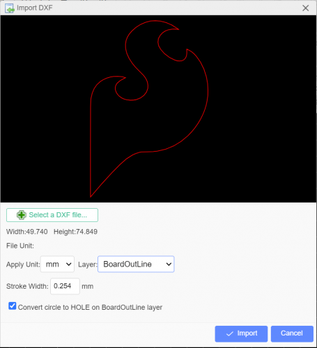
Import a .DXF for the Board Define
The very first thing you’ll have to do is locate some form that you really want your board to be: the easier the picture, the simpler will probably be to get a top level view from it. Then, take that picture into an enhancing software program of your alternative; I exploit Inkscape because it’s free to obtain and we don’t want a lot of bells and whistles for this, however something that permits you to generate a .DXF of your define will do!
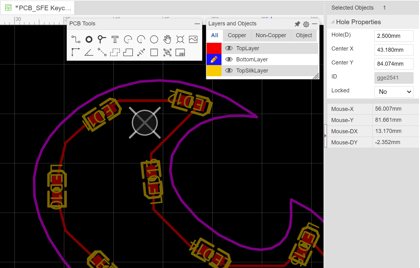
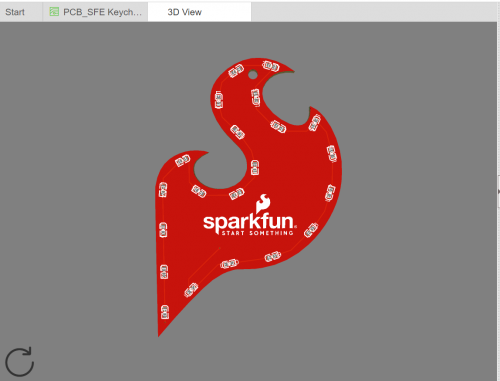
As soon as that’s able to go, generate your PCB and delete the default board define. Then, go as much as File → Import → DXF… and choose your file. A preview of the file will popup, with a dimension description beneath the ‘Choose a DXF File…’ button; one factor to remember is that JLCPCB has an extra cost for boards exceeding 100x100mm and the dimensions might be imported out of your DXF file. I needed mine to be keychain sized, so I made positive to notice that when creating the DXF of the define I needed (which appears vaguely acquainted, don’t it?). With the scale good to go, all that’s left is to make sure that our layer is ready to ‘BoardOutline’ within the dropdown menu.

Orienting Elements Alongside a Curve
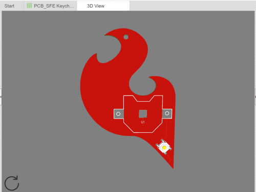
Now that the define is in, we will place and join our elements how we’d like! Since my board has these enjoyable curves, I needed to copy that form with my LEDs:
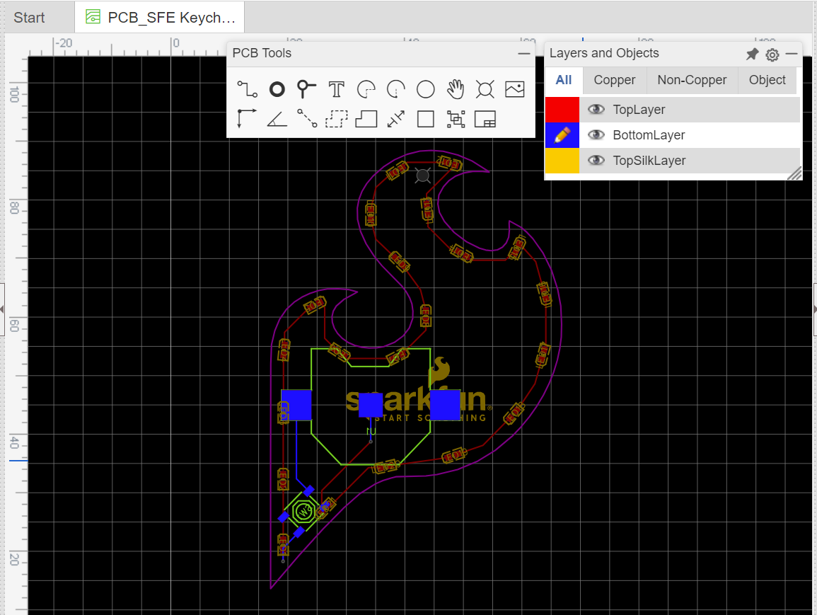
The best method to do that is to pick the half and drag the inexperienced dot round till it’s laying the way you need it. It’s also possible to choose the half and kind diploma values incrementally within the field labeled ‘Rotation’ on the proper facet of the designer.
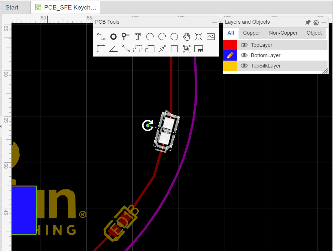
One factor to concentrate on when orienting components outdoors of 90 diploma increments is how you propose to position them when constructing the board. The best choice is to get them organized totally constructed from JLCPCB since they’ve bought all the flowery toys for manufacturing boards. Hand-placing, whereas time consuming, is an effective method to have the ability to management the orientation your self, however can get slightly complicated and is simple to bump components misplaced.
The final choice is to make use of a choose and place if in case you have one at your disposal. I’ve labored with the CHMT36VA from Appeal Excessive with curved half placements prior to now, and it did nice with them; I used to be constructing a whole lot of boards and did discover a little bit of drift over time, however it was a fast recalibrating and we had been again on observe! In the event you’re fascinated about studying extra about that machine, test it out right here:
Making a Customized Silk
Subsequent we’re gonna take a look at incorporating a {custom} silkscreen in your board; this course of is similar to the board define, the place you’ll navigate to File → Import → Picture… and choose your file (it’s also possible to simply choose the picture icon from the PCB instruments bar and that can open up the identical immediate window). Remember, when deciding on what you wish to add, that the silkscreen is a single coloration; taking part in with constructive and adverse house permits for lots of dynamic imagery, however can’t fairly do all of it.
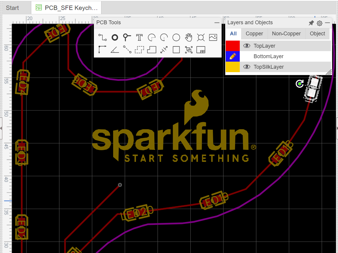
One final be aware with this: the pictures normally place on the TopLayer by default, so you should definitely choose it and alter the dropdown on the proper hand facet to ‘TopSilkLayer’, in any other case it’ll construct as a copper space and be coated by the solder masks. Which, you’d nonetheless be capable of see on the ultimate board, however will intervene together with your traces in the event that they occur to cross paths.
Including a Mounting Gap
Final up, we’re going to take a look at including a mounting gap to the board: these are nice for standoffs, screws, keyrings, just about something that attaches your board to one thing else. This can be a actually easy step, with a number of issues to notice; choose the circle with the X behind it from the PCB Instruments bar and place it wherever you’d like. By default, the diameter is 2.032mm and, relying on what you’re seeking to thread by means of it, you’ll be able to change this (with the half chosen) on the proper hand facet. For keyrings, I discover that bumping it as much as 2.500mm is kind of that Goldilocks zone. In the event you’re placing a screw or standoff by means of it, seize some calipers and measure your {hardware} to get a superb match.
Now, you’ll wish to take into account what materials goes by means of the board as nicely; though I didn’t with this design, if I had constructed out a copper space as a VCC or GND aircraft, working a chunk of steel by means of a gap within the board might find yourself shorting it out. In the event you’re utilizing copper areas it’s all the time a good suggestion to isolate round holes within the board simply in case. I had a keychain PCB I made some time again that ended up shorting from the damage of it transferring across the steel keyring over time; it was nonetheless enjoyable to have a look at however it didn’t mild up anymore, which is simply merely not as cool.
That’s all, of us!
Thanks all for becoming a member of me for this mini-series, and I hope you’re inspired to take a look at the vast world of PCB design. In the event you do find yourself dabbling in it, or going all out, please you should definitely share your tasks with us!
For these , right here’s the ultimate take a look at the 3D view of the board we had been working with:
Designing your personal PCB? Inform us the way it went within the feedback beneath, or present us on Twitter, Instagram, Fb or LinkedIn.