
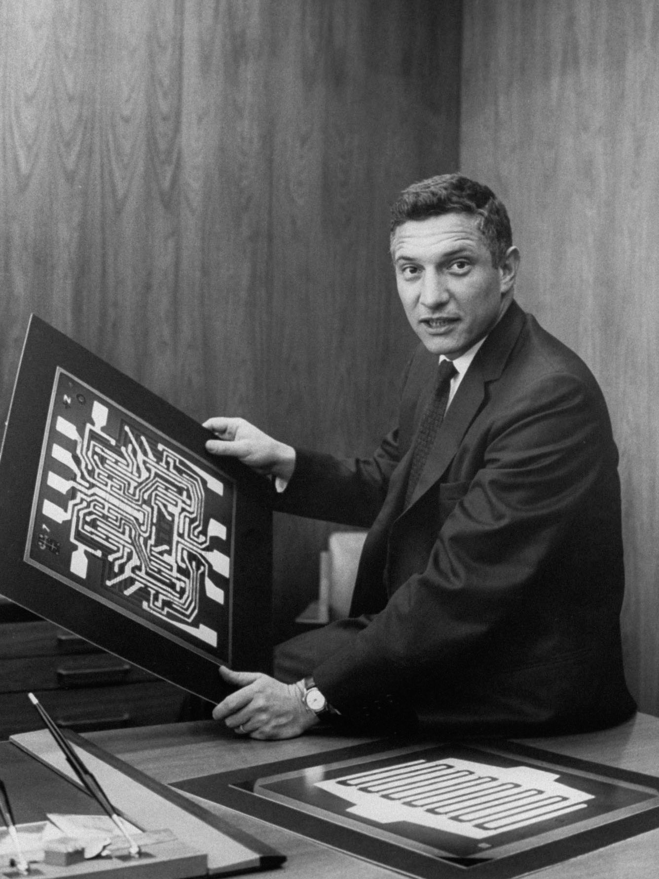
Lathrop had spent years trying by means of microscopes to make one thing small look greater. As he puzzled over find out how to miniaturize transistors, he and Nall puzzled whether or not microscope optics turned the other way up may let one thing large—a sample for a transistor—be miniaturized. To search out out, they lined a bit of germanium materials with a sort of chemical known as a photoresist, which they acquired from Eastman Kodak, the digital camera firm. Mild reacts with photoresist, making it both tougher or weaker. Lathrop took benefit of this function and created a “masks” within the form of a mesa, inserting it on the microscope with upside-down optics. Mild that handed by means of holes within the masks was shrunk by the microscope’s lens and projected onto the photoresist chemical substances. The place the sunshine struck, the chemical substances hardened. The place gentle was blocked by the masks, they might be washed away, leaving a exact, miniature mesa of germanium. A technique to manufacture miniaturized transistors had been discovered.
Lathrop named the method photolithography—printing with gentle—and he and Nall filed for a patent. They delivered a paper on the subject on the annual Worldwide Electron Units Assembly in 1957, and the Military awarded him a $25,000 prize for the invention. Lathrop purchased his household a brand new station wagon with the cash.
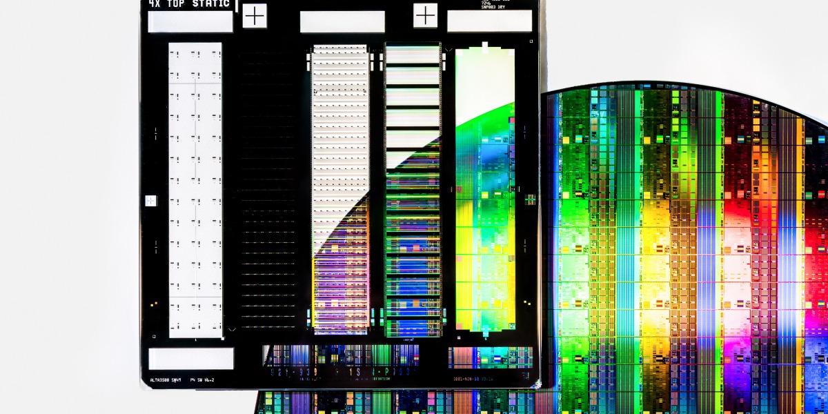
Within the midst of the Chilly Battle, the marketplace for mortar fuzes was rising, however Lathrop’s lithography course of took off as a result of corporations producing transistors for civilian electronics realized its transformative potential. Lithography not solely produced transistors with unprecedented precision but in addition opened the door to additional miniaturization. The 2 corporations main the race to industrial transistors—Fairchild Semiconductor and Texas Devices—understood the implications early on. Lithography was the instrument they wanted to fabricate transistors by the hundreds of thousands, turning them right into a mass-market good.
Portray with gentle
Robert Noyce, one of many cofounders of Fairchild, had studied alongside Lathrop when each had been PhD college students in physics at MIT. The 2 of them had spent their weekends in graduate college climbing New Hampshire’s mountains, they usually had stayed in contact after graduating. At Fairchild, Noyce moved shortly to rent Nall, Lathrop’s lab companion, and spearheaded his firm’s lithography efforts by jury-rigging his personal system with a set of 20-millimeter digital camera lenses he’d purchased from a Bay Space images store.
Lathrop, in the meantime, took a job at Fairchild’s competitor, Texas Devices, driving his new station wagon all the way down to Dallas. He arrived simply as his new colleague and lifelong pal Jack Kilby was getting ready to creating a bit of semiconductor materials with a number of digital parts constructed—or built-in—into it. These built-in circuits, it quickly turned clear, might be effectively produced solely with Lathrop’s lithography technique. As chip corporations strove to shrink transistors to cram extra of them onto chips, photolithography supplied the precision that miniaturized manufacturing required.
Fairchild and Texas Devices made their first lithography machines in home, however the rising complexity of the machines quickly attracted new entrants. As the size of transistors declined from centimeters to millimeters to microns, the significance of precision optics elevated. Perkin-Elmer was a Connecticut-based agency that produced specialised optics for the US army, from bombsights to spy satellites. Within the late Sixties, it realized that this experience might be used for lithography, too. It developed a scanner that would undertaking the masks sample onto a silicon wafer whereas aligning them with virtually flawless precision. The scanner then moved a light-weight throughout the wafer like a duplicate machine, portray it with strains of sunshine. This instrument proved able to fabricating transistors as small as a micron—one millionth of a meter.
TED STRESHINSKY/GETTY IMAGES
However the method wasn’t sensible as chip options obtained nonetheless smaller. By the late Nineteen Seventies, scanners started to get replaced with steppers, machines that moved gentle in discrete steps throughout a wafer. The problem with a stepper was to maneuver the sunshine with micron-scale precision, so that every flash was completely aligned with the chip. GCA, a Boston-based agency that had its origins in spy balloons, devised the primary stepper instrument, reportedly on the recommendation of Texas Devices government Morris Chang—later the founding father of TSMC, which is right this moment the world’s largest chipmaker.
New England’s specialist lithography corporations quickly confronted steep competitors. Within the Eighties, as Japanese chipmakers started profitable main market share within the manufacturing of reminiscence chips, they began shopping for from Nikon and Canon, two homegrown producers of lithography instruments. Across the identical time, the Dutch chipmaker Philips spun out its personal unit that made lithography instruments, calling the brand new firm ASML.